QFN stands for quad flat no-lead. It is a bottom-terminated surface-mount IC package with electrical terminals located on the underside, typically around the perimeter.
A typical QFN includes:
Eliminating projecting leads gives QFNs a smaller footprint than many leaded packages and shortens the connection between the package and PCB.
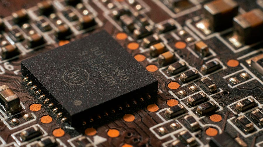
Quad flat no-lead (QFN) packages are common in designs where board space, electrical performance, and heat dissipation matter. Instead of leads that extend from the sides of the component, QFNs have electrical terminals on the underside of the package.
The design saves space, but it also puts most of the solder joints underneath the component, where they can't be inspected visually. Many QFNs also have a large exposed pad that affects footprint design, heat transfer, solder-paste deposition, and PCB assembly.
QFNs don't need the additional board area required for projecting gull-wing leads. Because the terminals are located underneath the package, the overall PCB footprint can be smaller than comparable leaded packages.
Their low package height also works well in products where vertical space is limited. These characteristics make QFNs useful in compact, high-density designs such as portable electronics, embedded systems, and other space-constrained assemblies.
Many QFNs use an exposed pad to move heat from the component into the PCB. When the device requires it, thermal vias beneath the pad can carry heat into internal copper planes or other copper areas of the board.-
The exposed-pad connection therefore needs to be considered as part of both the PCB's thermal design and its assembly process. The component manufacturer's recommendations should determine the pad geometry, connection, and thermal-via arrangement.
Compared with many leaded packages, QFNs can reduce package-to-PCB interconnect length and associated parasitic inductance. This is useful in RF / high-frequency PCB, power-management, and other performance-sensitive circuits.
QFNs work with standard SMT equipment and processes, including solder-paste printing, automated pick-and-place, and reflow soldering.
QFNs come in different sizes, terminal counts, pitches, and exposed-pad configurations. Some of the more common variations include:
The exact component matters more than the QFN category. The manufacturer's recommended land pattern should be used for the specific package being placed.
QFN footprint dimensions should come from the component manufacturer's recommended land pattern rather than from the package's nominal dimensions alone. Terminal pitch, exposed-pad geometry, solder-mask requirements, and other details can vary even between similar-looking QFNs.
PCB lands need to line up with the package terminals and provide enough solderable area to form reliable joints. Lands that are too small, too large, or incorrectly spaced can contribute to insufficient solder, bridging, and placement problems.
The exposed pad on many QFNs transfers heat from the component into the PCB. Depending on the device, it may also provide an electrical connection.
The component documentation should specify how the pad is connected and soldered. An exposed pad should not automatically be treated as a ground connection.
Thermal vias beneath the exposed pad carry heat into internal copper planes or other copper areas of the board. But an open via can also wick solder away from the exposed-pad joint during reflow.
Vias beneath the pad may be tented, plugged, filled, capped, or constructed as plated-over via-in-pad structures. The choice has to balance thermal performance and solder control with the fabrication process being used.
Via geometry and treatment can also influence solder distribution and voiding beneath the package.
Read more: PCB Via Types
Depending on the component, a QFN footprint may use solder-mask-defined or non-solder-mask-defined features. At finer terminal pitches, mask registration and minimum feature sizes become especially important.
The solder-mask design should follow the component recommendations while staying within the PCB fabricator's capabilities.
Pin 1 should be identified consistently in the PCB footprint, silkscreen, assembly drawing, and placement data. This is particularly important with square QFNs, where orientation may not be obvious from the package shape.
Read more: PCB Assembly Drawings: Polarities, Pin1 & Anode/Cathode Markings
Solder-paste volume has a direct effect on QFN joint formation. Too little paste can result in incomplete or open connections. Too much beneath the exposed pad can lift or tilt the package during reflow and interfere with the perimeter joints.
For a large exposed pad, the stencil opening is often divided into several smaller apertures rather than one large opening. This window-pane pattern provides better control over the amount and distribution of solder beneath the package and can help limit excessive voiding.
Stencil thickness and aperture geometry need to account for both the perimeter terminals and the exposed pad. The final design also needs to work with the solder paste and assembly process being used.

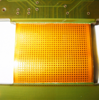
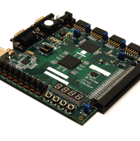
QFNs go through the same print, place, and reflow steps as other SMT components. The exposed pad and fine-pitch terminals are where process control becomes especially important.
A stencil deposits solder paste onto the PCB lands. Paste deposition needs to be consistent across the perimeter lands and exposed-pad area.
Pick-and-place equipment positions the QFN on the footprint. Molten solder provides some self-alignment during reflow, but accurate placement is still important, especially as package size and terminal pitch decrease.
The assembly passes through a controlled reflow profile. The solder paste melts and forms joints that provide the package's electrical connection and mechanical attachment to the PCB.
Inspection looks for misalignment, bridging, insufficient solder, voiding, and other defects. Because much of the joint is underneath the component, QFNs often require more than conventional optical inspection.
Some QFNs are moisture-sensitive and require controlled storage and floor-life management. Depending on their moisture-sensitivity classification and handling history, components may also require baking before assembly.
Moisture absorbed by the package can cause damage when the component is heated during reflow. The supplier's storage and handling requirements should be followed for the specific part.
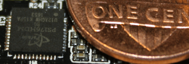
Integrated circuit in a Quad Flat No-Lead (QFN) package, featuring a compact, low-profile design
Voids are unfilled regions within a solder joint and are a particular concern beneath the large exposed pad used on many QFNs.
Some voiding is common. The amount, location, and effect on the soldered area determine whether it becomes a thermal or reliability concern. Paste deposition, via configuration, solder-paste characteristics, and reflow conditions can all influence void formation.
Fine terminal spacing leaves less room for excess solder between adjacent joints. Land geometry, stencil design, paste deposition, placement accuracy, and reflow conditions are common areas to investigate when bridging occurs.
Inadequate paste deposition can leave too little solder at the package-to-PCB interface. Open vias beneath the exposed pad can produce a similar result by allowing solder to wick into the via structure during reflow.
The location of QFN solder joints limits what can be checked with conventional optical inspection.
AOI can verify component presence, orientation, alignment, and any solder features that remain visible. Most joints beneath a conventional QFN are outside its view.
Packages with wettable flanks give AOI more to work with because the soldered side fillets are visible.
Read more: PCB Testing & Inspection
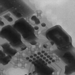
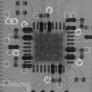
X-ray inspection can reveal information about exposed-pad solder distribution, voiding, bridging, and gross alignment that isn't available from a top-down optical view.
Conventional 2D X-ray still can't establish every aspect of perimeter-joint quality. Inspection criteria should reflect what the equipment can actually verify.
Read more: PCB Via Types
Reworking a QFN generally requires heating the component until its hidden solder joints reflow. Once the component is removed, the site is cleaned and prepared before the replacement QFN is positioned and soldered.
The process has to account for board thermal mass, nearby components, PCB land condition, and the temperature exposure of both the board and replacement part. Multiple thermal cycles can damage PCB lands or laminate, making controlled heating particularly important.
QFNs and QFPs both make connections around four sides of an IC, but QFPs use projecting gull-wing leads while QFN terminals sit beneath the package.
| Feature | QFN | QFP |
|---|---|---|
| Name | Quad Flat No-Lead | Quad Flat Package |
| Connection style | Bottom package terminals | Projecting gull-wing leads |
| PCB footprint | Generally smaller | Generally larger |
| Package-to-PCB electrical path | Generally shorter | Longer due to projecting leads |
| Thermal performance | Often includes an exposed thermal pad | Depends on package construction |
| Solder-joint visibility | Mostly hidden | Generally visible |
| Optical inspection | More limited | Relatively straightforward |
QFNs are useful where board space, thermal transfer, or short package-to-PCB connections are priorities. QFPs offer easier access to their leads for optical inspection and rework.
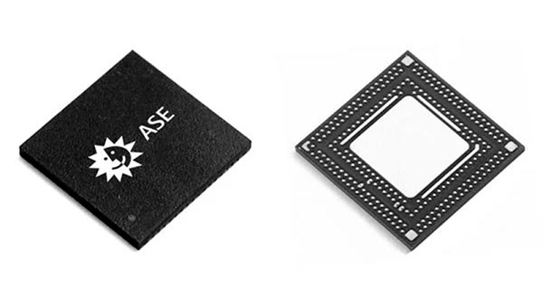
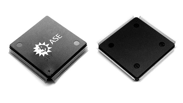
Images Source: https://ase.aseglobal.com/leadframe-packaging/
A QFN generally places flat terminals around the underside perimeter of the package, often with an exposed pad in the center. A ball grid array (BGA) instead distributes solder balls across the underside in an area array.
The area-array construction allows BGAs to accommodate higher interconnect counts. Both packages require careful footprint design and assembly control, although their land patterns and solder-joint structures are quite different.
Read more: BGA Assembly
QFNs appear in many types of electronics, including:
Their compact size makes them attractive for space-constrained designs, while the exposed-pad construction is useful in components that need an efficient path for moving heat into the PCB.
Before releasing a PCB design with a QFN, check:
QFNs combine a small footprint with good electrical and thermal performance, but their underside terminals and exposed pads put more weight on decisions made before assembly begins.
Footprint geometry, thermal vias, stencil design, and inspection should be reviewed together rather than as separate parts of the design. Problems such as bridging, voiding, insufficient solder, and solder wicking are far less expensive to catch at that stage than on assembled boards.
San Francisco Circuits provides PCB fabrication and assembly services for boards using QFNs and other surface-mount packages. Our team can review QFN footprints, thermal-via designs, stencil requirements, and inspection needs before production.
Contact San Francisco Circuits to discuss your PCB fabrication and assembly requirements.

PCB School
When designing a printed circuit board, one of the first decisions is choosing the appropriate IPC class. Specifying IPC Class 2 or Class 3 affects far more than a PCB's inspection criteria. The class chosen influences how the board is designed, fabricated, tested, and accepted throughout the manufacturing process. It also has a direct impact on cost, lead time, and the number of fabricators capable of producing the board.

PCB School
Standards like MIL-PRF-55110, MIL-PRF-50884, and MIL-PRF-31032 exist to enforce reliability, traceability, and performance in environments where failure isn't acceptable.

PCB School
Flying probe testing has been the golden standard of functional testing for low volume, prototype runs since the late 80s and 90s. It effectively flips the approach of the traditional in-circuit (ICT) bed-of-nails fixture test, where a custom-built frame with hundreds of spring-loaded pins contact test points simultaneously.
PCB School
Double-sided Ball Grid Array (BGA) assembly maximizes component density without increasing board size, enabling high-performance designs for applications ranging from smartphones and IoT devices to medical and industrial electronics.
PCB School
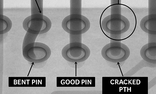
Managing strain during press-fit connector insertion is essential for high-density PCB reliability. Discover best practices and how San Francisco Circuits ensures reliable assembly for HDI, mil-spec, and medical applications.

PCB School
San Francisco Circuits covers the 8 types of PCB vias including blind, buried, microvias, through-hole, stacked, & thermal vias - what they are, how they work, & where they’re used in advanced PCB design.