Standards like MIL-PRF-55110, MIL-PRF-50884, and MIL-PRF-31032 exist to enforce reliability, traceability, and performance in environments where failure isn't acceptable.
Defense systems, aerospace applications, and hardware that operates in environments that would destroy a commercial board in weeks require more stringent standards than conventional applications.
MIL-PRF-31032 sets the bar highest, with the tightest process controls and certification requirements for the most demanding applications. MIL-PRF-50884 handles flex and rigid-flex constructions. MIL-PRF-55110 is an inactive spec for new designs, largely replaced with MIL-PRF-31032. 55110 guidelines covered qualification and performance for rigid boards.
Together, they give engineers a defined target and a common language for what a military grade circuit board needs to achieve.
Note: DLA has announced its intent to discontinue oversight of MIL-PRF-31032, MIL-PRF-55110, and MIL-PRF-50884 qualification programs unless another government organization assumes responsibility. Existing military PCB programs continue to utilize these specifications, and qualified manufacturing sources remain available.
Since 2005, San Francisco Circuits has been a trusted U.S. provider of advanced PCB manufacturing and assembly solutions for military spec boards.
For federal and defense projects, reliability is paramount. San Francisco Circuits adheres to stringent standards and guidelines, including NIST 800-171 cybersecurity guidelines and ITAR registered, ensuring that your mission-critical systems meet or exceed all regulatory requirements.
San Francisco Circuits sources boards through a curated network of DLA-qualified US-based manufacturing and assembly partners rather than a single in-house facility. For MilSpec programs, this means access to fabricators whose qualifications, process capabilities, and technology scopes are matched to the specific requirements of your design — rather than fitting your design to one shop's limitations


MIL-PRF-31032 is the modern, preferred standard covering all board types.
MIL-PRF-55110 handles legacy rigid PCB applications and MIL-PRF-50884 specifically governs flex and rigid-flex boards.
All three demand stricter process and material traceability, tighter dimensional tolerances, more rigorous defect rejection, and ongoing government oversight compared to commercial IPC Class 3 standards.
| Guideline Name | Technology | Official status | Practical status | Specification document |
|---|---|---|---|---|
|
MIL-PRF-31032 |
All board technologies |
Active - preferred for all new designs |
The current gold standard; covers rigid, flex, and rigid-flex under one QML umbrella. Required for new DoD contracts. Current revision: Rev D (March 2025) |
Download MIL-PRF-31032 |
|
MIL-PRF-50884 |
Flexible and rigid-flex PCBs |
Active - still valid for flex/rigid-flex |
Remains active; verification now accomplished via MIL-PRF-31032 slash sheets.
Current revision: MIL-PRF-50884G |
Download MIL-PRF-50884 |
|
MIL-PRF-55110 |
Legacy rigid PCBs |
Legacy - inactive for new design since Dec 1997 |
Remains active for legacy systems. No new product qualifications permitted unless also MIL-PRF-31032 approved.
Current revision: MIL-PRF-55110J |
Download MIL-PRF-55110 |
MIL-PRF-31032 is a performance specification, not a quality standard, that establishes general performance requirements and verification requirements for all printed circuit board types (rigid, flex, and rigid-flex).
Every single PCB produced for the military/DoD must be manufactured by a company certified to this specification, with no exceptions.
Key guidelines of MIL-PRF-31032 include:
Technical Review Board (TRB): PCB manufacturers must establish a TRB, submit PCB samples for qualifying their technology scope (validated every two years), and undergo ongoing monthly sampling of the most demanding MIL PCBs to a DLA-certified lab to maintain approval.
Technology Scope Limits: All PCBs built to MIL certification must be within the approved scope of technology and cannot exceed the approved technology by more than 25%. For example, if approved for 12-layer PCBs, a manufacturer is prohibited from building 20-layer MIL PCBs until additional approval is obtained.
Periodic Conformance Inspection (PCI / Group B): Conducted as required
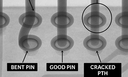
Plating & Voids: Copper plating thickness measuring less than 80% of the required thickness is treated as a void. A maximum of one void per panel is allowed, and it must not exceed 5% of the overall PCB thickness. No voids are permitted at the interface of the plated hole wall and the internal conductive layer.
Land Defects: External edge defects on surface mount lands must not exceed 20% of the land length and must not intersect the pristine area. Internal land defects must not exceed 10% of the length or width of the land.
Qualification Timeline: The full qualification process typically takes 12–18 months from initial application to DLA approval.
Download the full performance specification document:
MIL-PRF-31032D 1
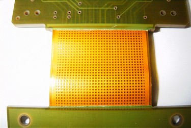
Rigid Flex PCB
MIL-PRF-50884 establishes the performance and qualification requirements for flexible and rigid-flex printed wiring boards, with or without plated-through holes. It classifies boards by type, covering single-sided flex, double-sided flex, and rigid-flex constructions.
Key guidelines of MIL-PRF-50884 include:
Soldering Durability: All current board types must be able to withstand five solder and unsoldering operations without degradation. This is a requirement that superseded the older single-operation standard from earlier revisions.
Rigid-Flex Transition Zone: The transition zone refers to the length of the rigid area as it extends and transitions to the flexible area. During manufacturing, flex coverlays may be extended so that lamination along the rigid area captures the flexible area to create a gapless transition.
Qualification Pathways: Manufacturers can qualify through either the QPL path (individual product qualification) or the QML path (qualifying an envelope of materials and processes rather than individual products), the latter being more suited to rapidly advancing technologies.
Design Standard: For boards that must meet MIL-PRF-50884 performance requirements, the IPC-2223 design specification is the recommended design reference.
Download the full performance specification document:
MIL-PRF-50884 2
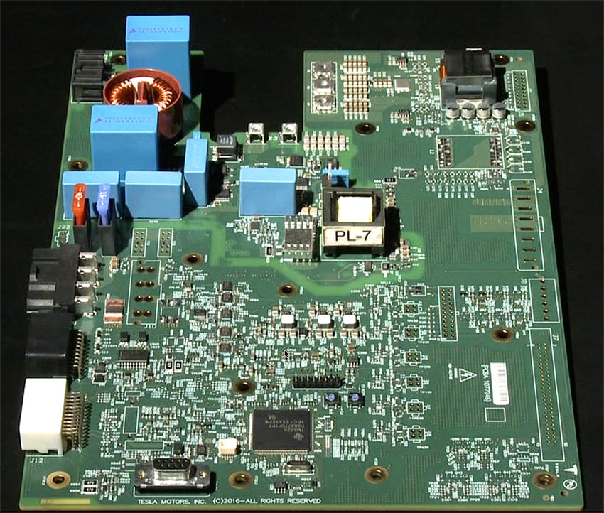
Assembled board with BGA and small components
MIL-PRF-55110 covers rigid single-sided, double-sided, and multilayer printed wiring boards. It has been marked "Inactive for New Design" since December 31, 1997, but remains in active use for legacy military programs. The specification uses a hierarchical type system, meaning qualifying for Type 3 automatically covers Type 1 and Type 2 boards.
Key guidelines of MIL-PRF-55110 include:
Annular Ring: Military specifications demand larger minimum annular ring margins than the 0.002″ minimum required by IPC Class 3.
Conductor Thickness: When a copper foil weight is specified, MIL-PRF-55110 allows up to a 10% reduction below the minimum allowable foil thickness to accommodate chemical or mechanical cleaning processes.
Surface Defects: It mandates strict rejection of minor surface imperfections like measling, crazing, and foreign material, even if they don't impact board performance, unlike IPC Class 3.
Qualification: Under the traditional QPL program, qualifications are validated every two years. Manufacturers using the QML pathway through MIL-PRF-31032 do not have expiration dates on their 55110 qualification but must maintain QML status through ongoing TRB reviews and DLA audits. You can no longer obtain new approval for 55110 unless you are already MIL-PRF-31032 approved.
Download the full performance specification document:
MIL-PRF-55110 3
Controlled Impedance
A ±5% tolerance is easy to hit in simulation, but maintaining it on a physical board requires consistency across multiple variables at the same time: dielectric thickness across lamination cycles, copper weight from panel to panel, and plating uniformity across the board.
Any of these can drift within acceptable ranges individually and still push impedance outside tolerance when combined. Test coupons are incorporated into production panels to verify impedance and stackup performance without risking critical traces.
Military specifications allow a range of approved materials, but mixed-material stackups require careful management of differences in thermal expansion coefficients, dielectric constants, and mechanical behavior under lamination. Material combinations that each meet spec individually can still produce stress concentrations or delamination risk that don't appear until fabrication or qualification testing.
DFM review against actual process capability (not just datasheet specs) is the standard way to catch these issues before production.
Read more in our PCB Material Reference Guide
Designs that combine several of the following push process control requirements at every fabrication step:
Aspect ratios at or near 15:1
Minimum hole sizes down to 0.004"
Multiple sequential lamination cycles
Mixed copper weights across layers
Sequential lamination cycles build up cumulative mechanical stress, and dielectric thickness variation, which is a normal artifact of any production environment, can shift impedance enough to push a board outside qualification limits on its own. What makes this particularly demanding is that each of these constraints may individually fall within spec, yet together they compress the available process window significantly.
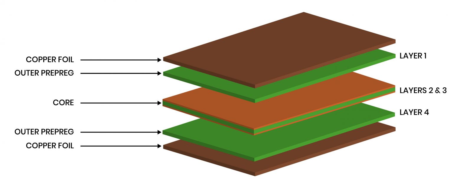
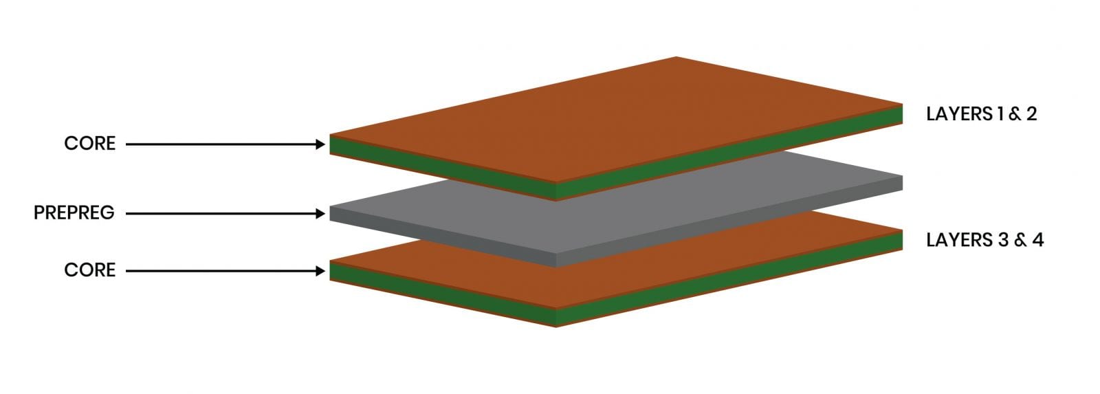
Your lamination method also matters. Foil construction is generally preferred for MilSpec work over cap construction due to better layer-to-layer registration and higher yield, particularly as layer count and complexity increase.
Copper plating thickness measuring less than 80% of the required minimum is treated as a void. A maximum of one void per panel is allowed, and it must not exceed 5% of the overall PCB thickness. No voids are permitted at the interface of the plated hole wall and the internal conductive layer.
See more in our PCB Stack-Up Guide with Examples
Use our PCB stackup calculator / design tool to help design and visualize your multilayer PCB stackup from 4 to 14 layers.
MilSpec requires testing and inspection beyond commercial IPC Class 3 standards.
The required tests include:
Microsection analysis: cross-sectioning drilled and plated holes to verify barrel thickness, annular ring integrity, and internal layer connections
Electrical continuity and isolation testing: performed on 100% of boards, not a sampled basis
Thermal stress testing: elevated temperature exposure to evaluate solder float resistance and laminate integrity
Visual and dimensional inspection: verified against the acceptance criteria in the applicable specification
Every test result must be documented and included in the board's traceability record.
Automatic Optical Inspection (AOI)
Military specifications set performance requirements for operating environments that commercial standards don't cover.
Boards must meet defined thresholds for:
Thermal cycling across wide temperature ranges
Humidity and moisture resistance
Vibration resistance
Shock loading, depending on the application
These requirements affect material selection, via design, and copper weight decisions at the design stage. A board that meets electrical and dimensional requirements at room temperature can still fail thermal cycling or vibration requirements if those parameters weren't part of the stackup and layout decisions.
MilSpec traceability requirements cover:
Material certifications
Process documentation
Inspection records
Chain-of-custody traceability for components
All documentation must be complete and consistent with the as-built board before it ships. Incomplete records, inconsistencies between documentation and what was actually built, or formatting that doesn't match program office requirements will hold shipment until corrections are approved. Documentation review cycles need to be part of the production schedule, not an afterthought.
MilSpec boards have mandatory marking requirements that differ from commercial standards. Manufacturer identification, date codes, specification compliance markings, and lot traceability information must appear on the board in defined formats. An unmarked or incorrectly marked board creates a documentation gap that holds up acceptance. Marking requirements need to be designed in and reviewed during DFM, not corrected after fabrication.
Example of a thru-hole power supply with its pins detailed in silkscreen.
Certified manufacturers can differ in process capabilities, preferred materials, reliable tolerance ranges, and DFM feedback practices while still meeting the same military specification. A design built around one fabricator's process window may need adjustments at another certified shop. Engaging fabrication at the stackup and initial layout stage lets material combinations, tolerances, and design features get validated against a specific manufacturer's actual process capability before the design is locked.
Military PCB specifications set the requirements for materials, dimensions, plating, testing, and documentation. How well a program meets them in production depends on decisions made long before the board reaches the fab house.
1 Defense Logistics Agency (DLA). MIL-PRF-31032: Performance Specification — Printed Circuit Board/Printed Wiring Board, General Specification For. U.S. Department of Defense. Accessed April 25, 2026. https://landandmaritimeapps.dla.mil/Downloads/MilSpec/Docs/MIL-PRF-31032/prf31032.pdf
2 Defense Logistics Agency (DLA). MIL-PRF-50884: Performance Specification — Printed Wiring Board, Flexible or Rigid-Flex, General Specification For. U.S. Department of Defense. Accessed May 8, 2026. https://landandmaritimeapps.dla.mil/Downloads/MilSpec/Docs/MIL-PRF-50884/prf50884.pdf
3 Defense Logistics Agency (DLA). MIL-PRF-55110: Performance Specification — Printed Wiring Board, Rigid, General Specification For. U.S. Department of Defense. Accessed May 8, 2026. https://landandmaritimeapps.dla.mil/Downloads/MilSpec/Docs/MIL-PRF-55110/prf55110.pdf

PCB School
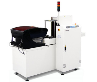
Flying probe testing has been the golden standard of functional testing for low volume, prototype runs since the late 80s and 90s. It effectively flips the approach of the traditional in-circuit (ICT) bed-of-nails fixture test, where a custom-built frame with hundreds of spring-loaded pins contact test points simultaneously.
PCB School
Double-sided Ball Grid Array (BGA) assembly maximizes component density without increasing board size, enabling high-performance designs for applications ranging from smartphones and IoT devices to medical and industrial electronics.
PCB School
Managing strain during press-fit connector insertion is essential for high-density PCB reliability. Discover best practices and how San Francisco Circuits ensures reliable assembly for HDI, mil-spec, and medical applications.

PCB School
San Francisco Circuits covers the 8 types of PCB vias including blind, buried, microvias, through-hole, stacked, & thermal vias - what they are, how they work, & where they’re used in advanced PCB design.

PCB School
Discover why NIST 800-171 compliance is essential for PCB manufacturers. As a PCB buyer, learn how this cybersecurity framework safeguards your sensitive data & ensure you are engaged with a boardhouse that meets these requirements.
PCB School
San Francisco Circuits covers board-level tips for the design & layout of high-speed circuits in advanced applications.
