Printed circuit board testing should be considered during all phases of production including design/layout, fabrication and assembly.
Whether it’s a simple bare board for continuity and netlist testing or functional test of an assembled board, tests are always strongly recommended.
We offer a wide variety of PCB testing and inspections for all boards we provide - both bare board fabrication and assembled PCBs.
The simplest board can still have issues and if untested, can cost a company significantly - both in time and budget.
It’s critical to test the product both in the early design stages and end-production in order to lower the chance of integration or field failures and prevent defects or issues early in the product life cycle.
An engineer can only control so much with regards to component tolerances, part-to-part variation, noise immunity/emission and general specifications or call-outs in a drawing for PCB fabrication or PCB assembly.
There are many things you can do to increase yields during production and confidently produce boards that will be reliable in a product. It all depends on the design specifications and what is needed to achieve a reliable circuit board.
The PCB design requirements that relate to speed, capacity (current/voltage), component size/complexity, temperature and overall performance should drive what tests happen during production.
There are two general kinds of tests:
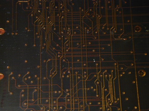
Bare board tests typically consist of the PCB manufacturer checking against netlists for “shorts” or “opens.”
The first step is DFM test (Design for Manufacturing) with software that runs design rule checks against GERBER files.
DFM checks the design for shorts or opens, which can be very helpful before board fabrication even happens. But once the board has been fabricated, a simple bare board electrical test can save major problems from happening downstream.
Visual Inspection. Visual inspection is a manual approach of testing that requires experienced inspectors who can determine what is acceptable and what is not. Visual inspections can be appropriate for the aesthetic or visual appearance of the board and can be checked by an individual.
What appears as poor solder mask application or scratches can later lead to failures of what is presently a good board.
Automatic Optical Inspection (AOI). AOI uses a vision system to capture an image of the circuit. By comparing this image to an expected image and to a set of design rules, image errors are detected. AOI machines detect flaws by a combination of design rule checks and comparison to design data.
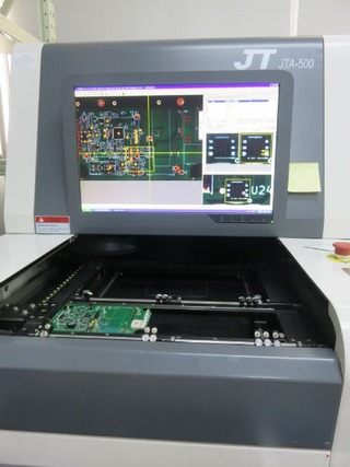
Automatic Optical Inspection (AOI)
TDR Impedance Test. More and more PCBs require impedance tests to ensure proper signal function. Impedance issues can cause performance and reliability problems that are easily detected through TDR (Time Domain Reflectometry) testing. The TDR test applies a very fast electrical step signal to the PCB or coupon through a controlled impedance cable and prone. Whenever there is a change in impedance value, part of the signal power is reflected back to the TDR tester. The data is recorded and saved by the TDR tester as well as graphed. The graph depicts the impedance values over the distance of the PCB or coupon under test. Data such as average, standard deviation, minimum and maximum values are also displayed.
Military PCB Inspection Group A. Group A inspection must be done by the manufacturing facility and includes the following:
Military PCB Inspection Group B. Group B inspection must be done by an outside laboratory (one that is recognized by the Department of Defense) and includes:
Microsections Inspection. Micro-sectional analysis, or cross-section analysis, is an advanced inspection method that examines the integrity of through-holes, laminate system, solder joint interfaces and other structures in and on the PCB.
Samples are extracted from the board and are then evaluated under high magnification.
Microsections analysis is a destructive procedure but can reveal critical defects of designs that are close to or exceed typical manufacturing specifications/tolerances - a test that is generally worthwhile for mass-production volumes of complicated boards. It is a required test for military PCB and Class 3 PCB requirements.
Electrical Test. Electrical testing is the most common methodology used to determine if a board is good or bad. To electrically test a board requires that the board come into physical contact with a measurement system. There are two test types performed: continuity and isolation.
Continuity testing checks for the continuous path or appropriate interconnect of pads, traces and through holes.
For isolation testing, we are trying to determine if networks or traces are separated or isolated from each other.
The type of test equipment appropriate to an operation varies with the type of boards produced, level of testing required and a variety of other influences.
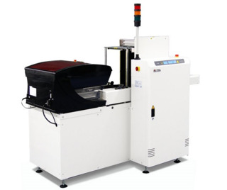
Most common test systems are Flying Probe testers. Each board requires the flying probe system to have unique programming (corresponding to the coordinates and test specs of each test point). As a result, this is a premium test but once configured and programmed, the testing process goes very quickly per board and, depending on annual volumes, is generally cost-effective in the long run.
Also, fixtured testers, with a dedicated test system and universal grid system, are used for testing medium to high-volume PCB production runs. A custom test fixture containing cabling/interfacing and systems that monitor specific signals could be well tailored to the design and test against high reliability and performance.
Hi Potential Testing (Hi Pot PCB Testing). Hi Pot testing is the opposite of a continuity test, where the testing system injects high voltage signals and verifies isolation between areas on the PCB, making sure that no current flows from one place to another.
This test is strongly recommended for high voltage circuit boards. Thin dielectrics sometimes go through Hi Pot PCB testing as well.
AOI (Automated Optical Inspection). Automated optical inspection systems can be placed into the production line just after the solder process. In this way they can be used to catch problems early in the production process. Process problems in the solder and assembly area can be seen early in the production process and the information can be used to provide feedback quickly to earlier stages.
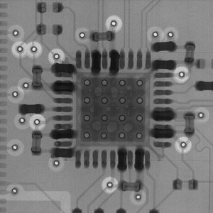
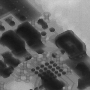
PCB X-Ray Testing. X-ray testing for PCBs are required when there are solder joints or leadless components whose pads are not visible via a microscope or the naked eye.
This is common for BGA and LGA footprints, which have pads underneath the component (BGA components come with pre-loaded solder balls underneath, which then flow and make a joint to the corresponding pad during the reflow process). While not required for all applications, it is highly recommended; if the board doesn’t work and you’re troubleshooting, you have no way of knowing whether it is or isn’t due to potential problems underneath the component.
X-ray testing for PCB prototypes is generally required.
Flying Probe Test. A flying probe system equipped with pogo-pin based probes injects and monitors signals via test pins on the boards. Read more about flying probe testing.
Functional Test. Functional testing is always the last gatekeeper in the manufacturing plan. It provides a go or no-go decision on finished PCBs.
It will test the final functionality of the product. This doesn’t test whether the board is good or not, whether the solder is there or not nor part tolerance.
A functional test tells you whether it works as it should - testing the entire product ensuring that everything works together and can communicate properly.
Manual/Visual Testing. Visual inspections of assembled PCBs help to quickly eliminate cosmetic defects and obvious process defects.
This includes inspection of solder paste after the paste printing process step, components after the component placement process step and solder joints after the solder curing process step.
If volumes and complexity are at a minimum, testing boards by hand could be a viable option that is more reasonably priced than flying probe and custom test fixtures. With a well written test procedure, an operator could know exactly what to probe/measure and what tolerances are acceptable.
Or EMAIL US to discuss & quote your project
