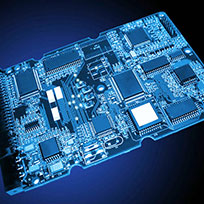
The computing industry has seen rapid growth over the past few years from personal computer devices like tablets and smartphones to high performance computing like crypto-mining and deep learning servers.
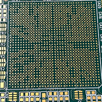
None of these advancements would be possible without ever-advancing PCB technology and HDI circuits staying ahead of this growth.
Your PCB fabrication and assembly partner needs to stay on top of board technology trends and meet industry standards for the highest level of computing possible.
As this industry continues to experience rapid growth, the manufacturing and design standards for computing electronics are consistently being updated and shifting. It is critical to work with a company who can manufacture bareboards and assemble PCB components to your specifications while also staying within standards, like those set by the IPC.
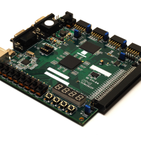
We've assisted in the design and assembly of many advanced computing applications. Just some possible applications and industries applicable to high-end computing are:
We can build at PCB prototype or production quantities, both bare-board and assembled boards.
| Specifications | Standard Technology | Advanced Technology |
|---|---|---|
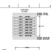
| Number of Layers |
1 - 12 |
14 - 40 |
| Quick Turn Times |
up to 24 hours for bare board fabrication or assembly (1-6 layers) |
|
| Minimum Board Thickness |
2 layer - 0.010" 4 layer - 0.020" 6 layer - 0.020" 8 layer - 0.062" 10 layer - 0.062" 12 layer - 0.062" |
2 layer - 0.005" 4 layer - 0.010" 6 layer - 0.031" 8 layer - 0.040" |
| Maximum Board Thickness |
2 layer - 0.125" 3-12 layer - 0.200" |
0.250" - 0.500" |
| Maximum Board Size |
16" x 22" 12" x 21"
|
10" x 16" 16" x 22" 12" x 21"
|
| Copper Thickness |
0.5 oz - 3 oz |
4 oz - 10 oz |
| Hole Aspect Ratio |
7 : 1 |
15 : 1 |
| Minimum Hole Size |
0.008" |
0.004" |
| Minimum Trace/Space |
0.006"/0.006" |
0.002"/0.002" |
|
Minimum Drill-to-Copper |
0.010" |
0.005" |
| Minimum Pitch |
1 mm |
0.3 mm |
| Final Finish |
HASL (Solder) Lead Free Solder Copper Gold Gold Fingers White Tin ENEPIG ENIG |
HASL Gold (ENIG/Hard/Soft) Selective Gold Immersion Silver OSP White Tin ENEPIG |
| Additional Features |
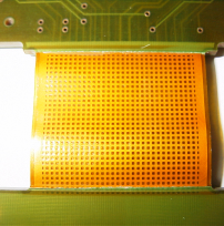
Plated Slots Non-plated Slots Controlled Dielectric Covered Vias Counter Sinks Counter Bores Dual Access Flex Suspended Leads |
Plated Edges Plated Milling Plated Counter Bores & Counter Sinks Edge Castellation Controlled Impedance Silver Filled Vias Non-Conductive Filled Vias
|
| Quality Standards |
IPC 6012 Class 2 Electrical Testing 100% Netlist Testing TDR Testing |
Milspec 31032 Milspec 55110 Milspec 50884 IPC 6012 Class 3 100% Netlist Testing TDR Testing |
| Special Technology |
|
Blind & Buried Vias Laser Drilled Vias Mechanically Drilled Micro Vias |
.png)
IPC is the trade association for the electronic interconnection industry. IPC provides industry standards for training, market research, public policy, and, most importantly, assembly and protection of electronic components.
IPC is a member-driven organization with over 3,000 member companies including designers, suppliers, board manufacturers, assembly companies, and original equipment manufacturers.
Meeting IPC standards for the computing industry affects the planning and designing of your PCB parts and even the testing and quality assurance of final PCBs.
San Francisco Circuits has provided computing PCB fabrication and assembly adhering to many standards for different uses within the industry. For example, all computing devices are tested by IPC-TM-650 standards.
IPC-TM-650 provides rules for evaluating PCBs in many categories.
Examine method IPC-TM-650 2.6.14.1, for example, provides how to test a board's propensity for surface electrochemical migration. This test determines the resistance to current flow over a PCB substrate surface. The IPC-TM-650-2.3.25.1 standard defines a technique for assessing the ionic cleanliness of bare printed wiring boards, which is significant since ionic contamination can cause problems that lead a PCB to fail.
With the majority of devices used in computing being interconnected and constantly communicating with one another it is best to closely follow good PCB practices. Standardized planning, designing, fabrication, and assembly are the key to compliant PCB components.
These help prevent board-level faults which could prevent compromising entire computing systems.
This makes following these best practices vital to the essential functions of the computing devices and the systems they are attached to:
Beyond the design and fulfillment process there are many stages of testing PCB components before being seen as the final product, including:
Catastrophic failures in the field can not only destroy the particular device the faulty PCB is in, but it could damage the other computing systems the PCB is interfacing with.
By taking the time to assess risks within each design with a thorough testing and inspection process, we are able to make sure that each potential hazard has been addressed and tested against.
Learn more about our PCB testing and inspection capabilities.
Our team of experts are ready to help get the right PCBs built for your computing devices and applications. Get a quote today for your next computing device or application.