Rigid flex printed circuit boards are boards that use a combination of flexible and rigid board technologies. Most rigid flex boards consist of multiple layers of flexible circuit substrates attached to one or more rigid boards externally and/or internally, depending upon the design of the application. The flexible substrates are designed to be in a constant state of flex and are usually formed into a flexed curve during installation.
Rigid flex designs are more challenging than the design of a typical rigid board environment, as these boards are designed in a 3D space, offering greater spatial efficiency. By being able to design in three dimensions, designers can twist, fold, and roll the flexible board substrates to achieve their desired shape for the final application's package.
To manufacture rigid flex PCBs, IPC offers advice and best practices. Technically speaking, rigid flex designs combine two or more conductive layers with flexible or rigid insulation in between them. The outer layers will then typically feature exposed pads or coverlay. Different from multi-layer flex circuits with stiffeners, the rigid layers will actually have conductors. Then plated through-holes will extend through both the flexible and rigid layers, with the exception of blind and buried vias. Because of those distinctions, rigid flex boards cost more than a standard circuit with stiffeners.
We can deliver rigid flex PCBs for complex multilayer commercial applications or high-reliability Mil-Spec printed circuit boards. Whatever your rigid flex requirements are, we can facilitate this process and ensure you get exactly what you need in a short amount of time.
Get your rigid flex PCBs turned fast.
| Specifications | Capabilities |
|---|---|
| Drill to copper – Outer layers | 8 mil |
| Drill to copper – Inner layers | 10 mil |
| Copper Thickness | 0.5 oz - 4 oz |
| Minimum Hole Size | 0.003" |
| Minimum Trace/Space | 0.003"/0.003" |
| Minimum Pitch | 0.5 mm |
| Copper to board edge | 0.007" |
| Coverlay Opening | 0.004" |
| Coverlay Web (Kapton) | 0.006" |
Rigid flexible PCBs offer a wide array of applications, ranging from military weaponry and aerospace systems to cell phones and digital cameras. Increasingly, rigid flex board fabrication has been used in medical devices such as pacemakers for their space and weight reduction capabilities. The same advantages for rigid flex PCB usage can be applied to military weaponry and weapon control systems.
In consumer products, rigid flex doesn't just maximize space and weight but greatly improves reliability, eliminating many needs for solder joints and delicate, fragile wiring that are prone to connection issues. These are just some examples, but rigid flex PCBs can be used to benefit nearly all advanced electrical applications including testing equipment, tools and automobiles. Not sure what technology needs to be used for your project? Call our experts and we can help you figure out whether you need rigid flex, flex PCB, RF PCB or other technology.
For smartphones and other portable devices, rigid designs without flexibility can provide certain complications. Rather than provide efficiency concerning space, it actually can hinder certain designs, leading to an increase in the device’s overall size. For devices that feature any sort of curvature, rigid boards won’t provide the necessary level of flexibility.
Whether producing a rigid flex prototype or production quantities requiring large scale PCB fabrication and PCB assembly, the technology is well proven and reliable. The flex PCB portion is particularly good in overcoming space and weight issues with spatial degrees of freedom.
Rigid flex designs feature both flexible and rigid layers in the design, which can add challenges and complications to the design stage. However, rigid flex can, in some cases, simplify designs with fewer parts with the elimination of wire harnesses and also connectors, when compared with rigid layouts.
Careful consideration of flex-rigid solutions and a proper assessment of the available options at the early stages in the design phase will return significant benefits in numerous design and manufacturing aspects. It is critical the PCB fabricator is involved early in the design process to ensure the design and fab portions are both in coordination and to account for final product variations.
The manufacturing phase is also more complex and time consuming than rigid board fabrication. All the flexible components of the rigid flex assembly have completely different handling, etching and soldering processes than rigid FR4 boards.
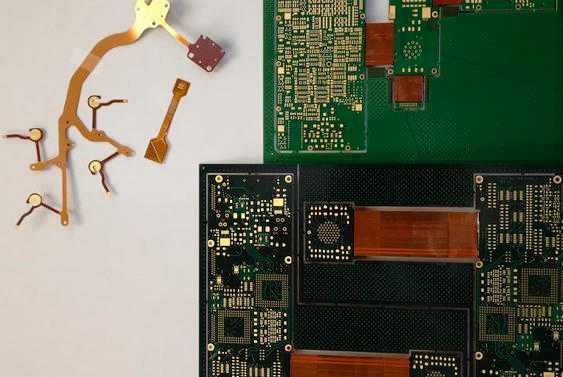
Rigid Flex PCB with Flex Substrate
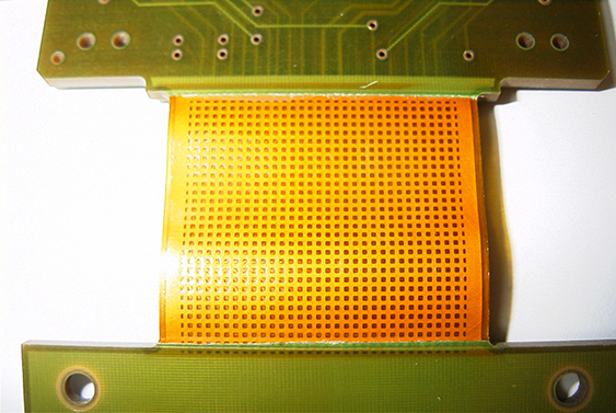
Rigid Flex PCB at Interconnect Point
Overall, rigid-flex PCBs require more extensive manufacturing and design stages than the alternative. The flexible sections need to be manufactured in a completely different manner than their rigid counterparts. Every flexible section between the rigid, needs to be laminated and sometimes drilled, and plated separately from the rigid sections, which leads to an increase in costs.
To properly assess rigid flex during the PCB design process, certain considerations must be taken into account for final product size variations. In the manufacture of rigid flex boards, the flexible polyimide core will shrink once the bonded copper foil is etched away.
The final assembly process requires the flex portions to be bent into shape, stressing the flex with the potential to cause fractures.
This additional stress can be addressed with some particular design choices, such as designing route traces through bent areas, avoiding placing vias near the flex rigid transition, crosshatch copper fill, and staggered parallel routing.
We are experts in rigid flex fabrication. Call us for help in the design process: 800.SFC.5143 or chat with our expert staff.
