Double-sided Ball Grid Array (BGA) assembly maximizes component density without increasing board size, enabling high-performance designs for applications ranging from smartphones and IoT devices to medical and industrial electronics.
BGA technology revolutionized PCB assembly by replacing traditional pins with solder balls beneath the package, allowing higher pin counts in a smaller footprint. Double-sided BGA assembly extends this concept by placing BGAs on both the top and bottom layers of the PCB, effectively increasing the usable board area and enabling more compact, complex designs.
The primary advantage of double-sided assembly is space efficiency. By utilizing both sides of the PCB, component density can increase significantly, often up to 50% compared to single-sided layouts, without enlarging the board footprint. This capability is critical in devices where miniaturization and performance are equally important.
But like any innovation, it comes with its share of hurdles.
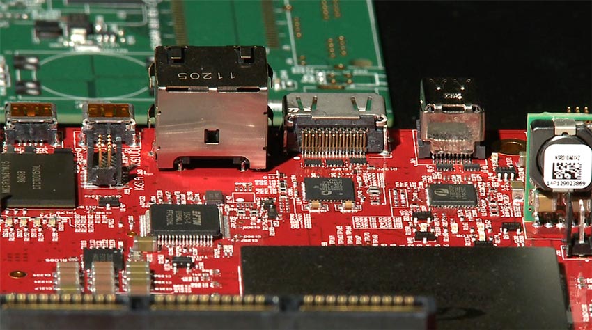
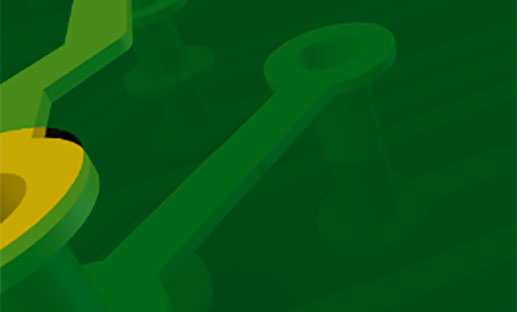
Crossection BGA with solder on PCB
One of the first stumbling blocks in double-sided assembly is simply agreeing on what to call the sides. Terms like “top” and “bottom” can cause confusion depending on the board’s orientation in the final product. Some prefer “primary” and “secondary” sides, aligning with CAD designs, while others opt for “first” and “second” to emphasize the soldering sequence.
At San Francisco Circuits, we follow IPC standards and refer to “solder source” and “solder destination” during process planning. This approach prioritizes the mechanics of assembly over arbitrary labeling, reducing the risk of errors.
Double-sided BGA assembly isn’t a one-and-done affair; it’s a carefully orchestrated sequence. Typically, the process involves surface-mount technology (SMT) with reflow soldering, where the board passes through an oven to melt solder paste and secure components, requiring careful thermal management.
The standard workflow typically includes:
For PCB prototype runs, selective soldering or hand assembly may be used for heavier components to reduce the risk of drop-off or thermal stress.
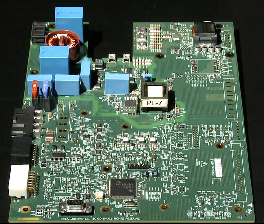
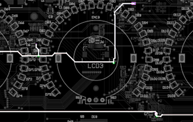
Assembled board with BGA and small components
Double-sided BGA assembly introduces several technical challenges:
Many hurdles are surmountable with smart strategies and process control:
Substrate Selection
Opt for high-Tg substrates (>170°C) that can withstand multiple reflow cycles to combat warpage. Read more about PCB material selection.
Component Sequencing
Design with offset BGAs where possible; mirroring works for identical packages but demands HDI builds with blind/buried vias. For mismatched sizes, solder lighter BGAs first on the bottom, heavier on top to minimize drop risks.
Reflow Profiling
Optimize temperature ramps for surface finishes (ENIG, ENEPIG) to prevent brittle intermetallic formation. Studies like those from the IOP Conference Series emphasize profiling to control intermetallic growth.
Inspection and Testing
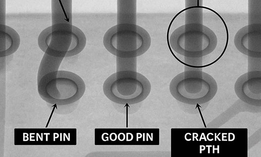
Consider asking your PCB assembler to implement X-ray imaging for hidden joints and electrical testing for functional integrity post-assembly.
By combining design-for-manufacturing principles with precision assembly processes, San Francisco Circuits delivers reliable double-sided BGA boards capable of supporting high-density, high-performance electronics.
At San Francisco Circuits, we provide more than manufacturing; we’re your partner in pushing electronic boundaries. With expertise in advanced PCB assembly, from quick-turn prototypes to full production runs, we ensure your double-sided BGA designs thrive.
Ready to elevate your project? Contact us today for a consultation. Let’s build the future, one solder ball at a time.
PCB School
Standards like MIL-PRF-55110, MIL-PRF-50884, and MIL-PRF-31032 exist to enforce reliability, traceability, and performance in environments where failure isn't acceptable.
PCB School
Flying probe testing has been the golden standard of functional testing for low volume, prototype runs since the late 80s and 90s. It effectively flips the approach of the traditional in-circuit (ICT) bed-of-nails fixture test, where a custom-built frame with hundreds of spring-loaded pins contact test points simultaneously.
PCB School
Managing strain during press-fit connector insertion is essential for high-density PCB reliability. Discover best practices and how San Francisco Circuits ensures reliable assembly for HDI, mil-spec, and medical applications.
PCB School
San Francisco Circuits covers the 8 types of PCB vias including blind, buried, microvias, through-hole, stacked, & thermal vias - what they are, how they work, & where they’re used in advanced PCB design.

PCB School
Discover why NIST 800-171 compliance is essential for PCB manufacturers. As a PCB buyer, learn how this cybersecurity framework safeguards your sensitive data & ensure you are engaged with a boardhouse that meets these requirements.
PCB School
San Francisco Circuits covers board-level tips for the design & layout of high-speed circuits in advanced applications.
