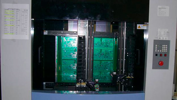
Flying probe testing has been the golden standard of functional testing for low volume, prototype runs since the late 80s and 90s. It effectively flips the approach of the traditional in-circuit (ICT) bed-of-nails fixture test, where a custom-built frame with hundreds of spring-loaded pins contact test points simultaneously.
With the flying probe test, the probes move and the board doesn’t.
Multiple programmable probes (typically 4–8) navigate to coordinates, contact pads, or vias to run continuity and isolation checks, verify component values, confirm polarity, and exercise power rails. The fixture, in effect, is software.
Change the design? Update the program. No new hardware.
Instead of requiring custom fixtures and extensive physical access, a flying probe test adapts to the board’s existing layout. It enables electrical validation for complex, dense, or lower-volume designs without forcing unnecessary redesign.
It’s slower (often on the order of 1–10 minutes per board instead of a 5–30 second ICT cycle) but for prototypes, low-volume production, and geometries that make fixtures impractical, it’s often the only rational option.
Until the design starts pushing limits.
Flying probe tests are ideal for prototypes, low-volume builds, design revisions, and geometrically complex boards where fixtures are either impractical or uneconomic. FPT can be done on bareboards and assembled boards. It has limits—especially around speed, hidden nets, and high-frequency behavior—but it also unlocks coverage that would otherwise be impossible.
When boards push technological constraints—HDI stackups, rigid-flex systems, RF-sensitive layouts, multi-board assemblies—flying probe becomes part of a broader strategy built around layered validation, not a silver bullet.
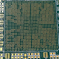
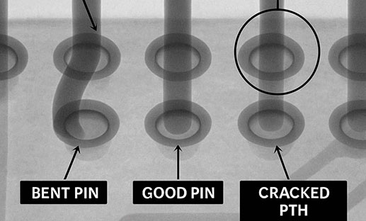
Many flying probe systems work best when test pads are at least around 10–20 mil in size with comparable spacing, and some shops prefer 16 mil or more between targets depending on their equipment and risk tolerance. Now design around 0.4 mm BGAs, dense QFPs, and tightly packed analog routing. Your potential test points are buried under components, squeezed between solder mask dams, or spaced on a grid no probe can reliably hit.
The fix isn’t “buy a better tester.”
The fix is designing for test from the beginning:
If you can’t test it, you can’t verify it. And unverified boards don’t ship.
ATG Flying Probe Test for Bare Boards
| In-Circuit Testing (ICT) | Flying Probe Testing (FPT) | |
|---|---|---|
|
Ideal Use Cases |
Production runs |
Prototypes |
|
Suitable for |
Bare Boards |
Bare Boards |
|
Hardware & fixtures |
Bed-of-nails custom-built frame fixture |
Fixtureless moving probe system (programmable probes, universal holders) |
|
Start-up Time |
Long: requires fixture design, fabrication, and debug; days to weeks |
Short: requires probe program from Gerbers/CAD; minutes to 1–2 days |
|
Testing Speed |
Fast: 5 sec to 2 min/board depending on complexity |
Slower: 2 to 30 min/board depending on complexity |
|
Cost per Board (high volume) |
Low |
Higher |
|
Design Change Flexibility |
Low - fixture redesign often required |
High - software update is sufficient |
|
Fault Testing Coverage |
High coverage for:
Key differences: |
High coverage for:
Key differences: |
|
Advanced Fault Detections |
Fixture-assisted pressure and powered measurements |
Phase Difference Measurement (PDM), high voltage stress, micro-short detection |
|
Access Requirement |
Requires dedicated test pads and fixture accessibility |
Can probe smaller or harder-to-reach points |
|
Mechanical Stress on Board |
High simultaneous contact force |
Low localized contact force |
|
Programming Effort |
Medium to high (fixture + test development) |
Medium (CAD/probe path generation) |
|
Failure Diagnostics |
Very fast pass/fail + node isolation |
Very detailed node-by-node diagnostics |
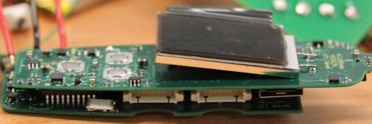
Rigid-flex PCBs are elegant – until assembly hides half your test access.
Example: A medical wearable uses an 8-layer rigid-flex stack with BGAs on both sides, RF shielding, and flex tails that fold into enclosure channels. The original assumption: probe post-assembly.
Reality: once it folds and closes, half the access vanishes.
The working strategy becomes staged testing:
No single method covers everything. The combination does.
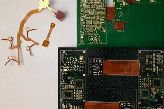
Rigid Flex PCB with Flex Substrate
.png)
High-frequency layouts don’t tolerate random stubs or parasitics. Every extra via risks disrupting impedance. Every additional test pad or stubbed branch becomes a potential antenna or reflection point.
So you adjust the strategy.
Continuity and isolation on power, control lines, and low-speed digital? Flying probe handles that cleanly.
Six GHz RF trace performance and matching? That’s vector network analyzer or RF functional validation after assembly – not a pogo-pin guess on a sensitive microstrip.
Not every net requires direct electrical probing. The goal isn’t theoretical coverage. It’s verified performance where it actually matters.
Read more about RF PCBs here.
Microcraft Flying Probe Test for Bare PCBs
Stacked assemblies create access dead zones. Once boards are mated, connector pins disappear under plastic, metalwork, and shields.
The solution is sequencing:
Some designs include breakaway flex tails or temporary access tabs specifically for probing before final assembly. That isn’t over-engineering.
That’s acknowledging reality.
Stacked PCBs
The layout is finished but DFM review flags insufficient access. The engineering team scrambles to squeeze pads into leftover clearance.
By then, you’re negotiating with a locked design.
The better approach is to define your test strategy at the schematic phase.
Impedance-controlled and precision analog circuits don’t tolerate random stubs and stray copper. In some regions, electrical probing simply isn’t viable.
When that happens:
A small replicated structure, isolated from the live circuit, gives you impedance and process verification without compromising the traces that actually carry your signals. You’re already fabricating the board, so use that to your advantage.
No single method covers everything.
Complex boards typically require:
Each catches different failure modes.
Read more about PCB testing & inspections here.
Flying probe is flexible, but not universal.
For stable, high-volume production, fixtures eventually win economically once the design is frozen.
Flying probe excels when flexibility matters more than raw speed: early prototypes, engineering builds, frequent revisions, and geometries that make fixtures risky or uneconomical.
That’s why with every prototype or production bare board fabrication order with us, flying probe testing is mandatory and included.
As a “high-touch” supplier, we pride ourselves on being part of your boards at every stage of production. As a PCB fab and assembly provider that specializes in complex boards, our engineers have solved versions of your problem before.
Involving test engineering during DFM and schematic review allows us to:
If your board is dense, stacked, RF-sensitive, or revision-heavy, test strategy can’t be an afterthought. Whether that means flying probe, hybrid inspection, staged testing for rigid-flex, or fixture-based ICT at scale, the goal is simple: eliminate surprises before fabrication, not after assembly.
If you’re facing a design that another shop labeled “untestable,” or you want to make sure yours never earns that label, start the conversation before physics forces one.
PCB School
Standards like MIL-PRF-55110, MIL-PRF-50884, and MIL-PRF-31032 exist to enforce reliability, traceability, and performance in environments where failure isn't acceptable.
PCB School
Double-sided Ball Grid Array (BGA) assembly maximizes component density without increasing board size, enabling high-performance designs for applications ranging from smartphones and IoT devices to medical and industrial electronics.
PCB School
Managing strain during press-fit connector insertion is essential for high-density PCB reliability. Discover best practices and how San Francisco Circuits ensures reliable assembly for HDI, mil-spec, and medical applications.

PCB School
San Francisco Circuits covers the 8 types of PCB vias including blind, buried, microvias, through-hole, stacked, & thermal vias - what they are, how they work, & where they’re used in advanced PCB design.

PCB School
Discover why NIST 800-171 compliance is essential for PCB manufacturers. As a PCB buyer, learn how this cybersecurity framework safeguards your sensitive data & ensure you are engaged with a boardhouse that meets these requirements.
PCB School
San Francisco Circuits covers board-level tips for the design & layout of high-speed circuits in advanced applications.