Have you ever submitted a Gerber file only to have a laundry list of feedback and red-pen markup sent back to you, creating hours of revisions and delays for the engineering team?
Delays like these not only increase the lead time of your product but increase costs, especially if special ordered materials are required for the adjustments.
Every PCB manufacturing facility has different PCB tolerances that affect an engineer’s target impedance and stack up.
While not mandatory, it is extremely beneficial for the PCB designer to consult the PCB manufacturer and PCB assembly shop as early as possible in the design and layout process to get a copy of the PCB tolerance requirements and stack up.
Use our PCB stackup calculator / design tool to help design and visualize your multilayer PCB stackup from 4 to 14 layers.
One of the benefits of working with a supplier like San Francisco Circuits is everything is managed under one roof - sales, engineering consultations, fabrication, component sourcing, and assembly.
Our specialty is in providing solutions to the most complex design challenges and ultra-demanding applications - be that high-heat, critical-reliability, or military standards.
We supply these advanced technologies to you, transforming the old way you would order printed circuit boards; with us, there is no more need to manage multiple supplier relationships and account for miscommunication on aspects like component overages or tolerances.
During your design process, follow these printed circuit board tolerance guidelines to ensure the quality (and feasibility) of the manufactured PCBs is maximized.
All of our circuit boards are built within valid IPC guidelines and standards, typically IPC-A-600 Class 2 standards. We can also build HDI boards with smaller tolerances upon request.
| Tolerances | Standards | Detailed Tolerance Standards |
|---|---|---|
| Inner Layer Clearances | 0.010" | |
| Pad Size | ±20 % |
IPC-6012 3.5.4.2.1 Rectangular Surface Mount Lands Defects such as nicks, dents, and pin holes along the external edge of the land shall not exceed 20% of either the length or width of the land for Class 2 or Class 3 boards, or 30% for Class 1, and shall not encroach the pristine area, which is defined by the central 80% of the land width by 80% of the land length as shown in Figure 3-6. Defects internal to the land shall not exceed 10% of the length or width of the land for Class 2 or Class 3 boards, or 20% for Class 1, and shall remain outside of the pristine area of the surface mount land. One electrical test probe ‘‘witness’’ mark is allowed within the pristine area for Class 1, 2 and 3.
IPC-6012 3.5.4.2.2 Round Surface Mount Lands (BGA Pads) Defects such as nick, dents and pin holes along the edge of the land shall not radially extend towards the center of the land by more than 10% of the diameter of the land for Class 1, 2 or 3 boards and shall not extend more than 20% around the circumference of the land for Class 2 or 3 boards or 30% for Class 1 as shown in Figure 3-7. There shall be no defects within the pristine area which is defined by the central 80% of the land diameter. One electrical test probe ‘‘witness’’ mark is allowed within the pristine area for Class 1, 2 and 3. |
| Hole Size | Standard Plated ±3 mils - Advanced Plated ±2 mils - NPT ± 1 mil - NPT > 126 mils ±2+ mils | |
| Printed Circuit Board Thickness | >=31 mils 10% or ± 3 mils which ever is larger - Thickness < 31 mils ±3 mils - Advanced 5% | |
| Rout (Board Outline & Internal Cutouts) | Standard ±10 mils - Advanced ±5 mils - Special ±3 mils | |
|
Copper Trace Width/Spacing
View More |
±20 % | IPC-6012 3.5.1 Conductor Width and Thickness When not specified on the master drawing the minimum conductor width shall be 80% of the conductor pattern supplied in the pro-curement documentation. When not specified on the master drawing, the minimum conductor thickness shall be in accordance with 3.6.2.12 and 3.6.2.13. 3.5.2 Conductor Spacing The conductor spacing shall be within the tolerance specified on the master drawing. Minimum spacing between the conductor and the edge of the board shall be as specified on the master drawing. If minimum spacing is not specified, the allowed reduction in the nominal conductor spacings shown in the engineering documentation due to processing shall be 20% for Class 3 and 30% for Class 1 and 2 (minimum product spacing requirements as previously stated apply). |
| OVERALL BOARD FEATURES | ||
| Minimum Inside Radius | 16 mils | |
| Controlled Impedance | Standard 10% - Advanced 5% | |
| Outer Copper Thickness | Absolute copper min. for 1/2 oz = 0.606 mils for 1 oz = 1.217 mils for 2 oz = 2.429 mils | |
| Minimum Width Between Profile & Copper | 5 mils | |
| SCORING | ||
| PCB Dimension X/Y | 10 mils | |
| Scoring Depth | ±3 mils on a 62 mil thick board | |
| Rigid PCB Thickness | >=31 mils 10% or ± 3 mils which ever is larger - Thickness < 31 mils ±3 mils - Advanced 5% | |
| Flexible PCB Thickness | ±1 mils | |
| Flexible Part Thickness | ±1 mils | |
| Flexible Part + Stiffener Thickness | ±1 mils | |
| BOW & TWIST | ||
| Bow & Twist Tolerance - with & without SMD | 0.75% | IPC-6012 3.4.3 Bow and Twist Unless otherwise specified in the procurement documentation, when designed in accordance with 5.2.4 of IPC-2221, the printed board shall have a maximum bow and twist of 0.75% for boards that use surface mount components and 1.5% for all other boards. Panels which contain multiple printed boards which are assembled on the panel and later separated shall be assessed in panel form. Bow, twist, or any combination thereof, shall be determined by physical measurement and percentage calculation in accordance with IPC-TM-650, Method 2.4.22. |
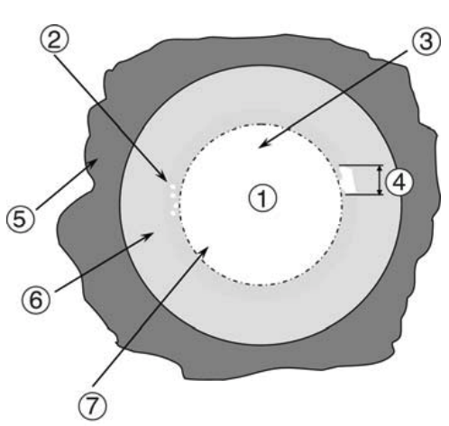
Figure 3-6 Round Surface Mount Lands
This image is Copyright 2019 by IPC International, Inc. and is used with IPC’s permission. This image may not be altered or may not be used by any other persons, companies or organizations other than the original user.
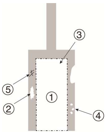
Figure 3-7 Printed Board Edge Connector Lands
This image is Copyright 2019 by IPC International, Inc. and is used with IPC’s permission. This image may not be altered or may not be used by any other persons, companies or organizations other than the original user.
