Medical devices have one crucial requirement - 100% reliability. When a patient’s health and life are at stake, nothing less than perfect functionality without failure is acceptable.
To achieve this level of reliability, your PCB manufacturer and assembly partner needs to meet and understand the various strict medical standards.
Medical standards have been in place for decades to guide the robustness and safety requirements of electronic designs. These standards are strict and can be challenging to meet so it’s important to verify your boardhouse’s credentials and protocols.
The largest governing bodies publishing medical device regulations are the IEC and the ISO. In addition, the FDA and FCC may also have their own standards. There are several different standards that are all necessary due to the broad scope a medical device may fall into.

San Francisco Circuits has provided medical PCB manufacturing and assembly that have adhered to many standards for different uses. Typically, all medical devices will be compliant with ISO 13485.
ISO 13485: ISO 13485 is used by organizations involved in the design, production, installation and servicing of medical devices. ISO 13485 is the FDA’s mandatory quality management system (QMS) for medical devices.
We have built or collaborated on many different types of medical device applications. Some devices and areas of interest we have built or collaborated on include:
Our team has the ability to provide PCB prototypes or production quantities, both bare-board and assembled, for whatever stage in your medical device development process you’re in.
Medical technology companies rely on our expertise in bridging the gap between their device’s concept into reality. Whether the requirements call for extreme miniaturization or fine line trace and space, medical companies select us because they know they can challenge us to push the boundaries beyond standard printed circuit technologies.
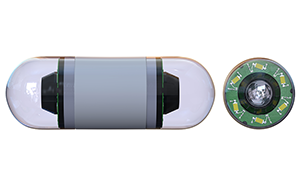
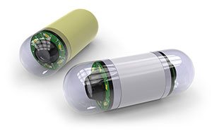
Pill Camera Medical Industry PCB Example
| Specifications | Standard Technology | Advanced Technology |
|---|---|---|
| Number of Layers |
1 - 12 |
14 - 40 |
| Quick Turn Times |
up to 24 hours for bare board fabrication or assembly (1-6 layers) |
|
| Minimum Board Thickness |
2 layer - 0.010" 4 layer - 0.020" 6 layer - 0.020" 8 layer - 0.062" 10 layer - 0.062" 12 layer - 0.062" |
2 layer - 0.005" 4 layer - 0.010" 6 layer - 0.031" 8 layer - 0.040" |
| Maximum Board Thickness |
2 layer - 0.125" 3-12 layer - 0.200" |
0.250" - 0.500" |
| Maximum Board Size |
16" x 22" 12" x 21"
|
10" x 16" 16" x 22" 12" x 21"
|
| Copper Thickness |
0.5 oz - 3 oz |
4 oz - 10 oz |
| Hole Aspect Ratio |
7 : 1 |
15 : 1 |
| Minimum Hole Size |
0.008" |
0.004" |
| Minimum Trace/Space |
0.006"/0.006" |
0.002"/0.002" |
|
Minimum Drill-to-Copper |
0.010" |
0.005" |
| Minimum Pitch |
1 mm |
0.3 mm |
| Final Finish |
HASL (Solder) Lead Free Solder Copper Gold Gold Fingers White Tin ENEPIG ENIG |
HASL Gold (ENIG/Hard/Soft) Selective Gold Immersion Silver OSP White Tin ENEPIG |
| Additional Features |
Plated Slots Non-plated Slots Controlled Dielectric Covered Vias Counter Sinks Counter Bores Dual Access Flex Suspended Leads |
Plated Edges Plated Milling Plated Counter Bores & Counter Sinks Edge Castellation Controlled Impedance Silver Filled Vias Non-Conductive Filled Vias
|
| Quality Standards |
IPC 6012 Class 2 Electrical Testing 100% Netlist Testing TDR Testing |
Milspec 31032 Milspec 55110 Milspec 50884 IPC 6012 Class 3 100% Netlist Testing TDR Testing |
| Special Technology |
|
Blind & Buried Vias Laser Drilled Vias Mechanically Drilled Micro Vias |
.png)
We can turn your flex circuits in 24 hours. View capabilities including .003" min. trace & space.
We can turn your rigid flex PCBs in 7 days with .006" min hole size & .003" min. trace/space.
24 hour quick-turn, turn-key, partial turn-key & consignment assembly with 01005 parts.
It’s always best to follow good practices with PCB layout to prevent board-level faults. In the case of medical devices, lives are dependent on the successful operation of the PCB, so following best practices is not just recommended, but essential.
Some of the best practices for medical PCB devices include:
In addition to the design process, there must be many stages of testing including:
And for PCB-specific tests, here are few important tests:
Though verification and validation tests may reveal some issues upfront before launch, failures in the field can be devastating. Thus, it’s best to increase overall confidence, test as thoroughly as possible, and to re-visit the risk assessment to make sure that each potential hazard has been addressed and tested against.
Learn more about our PCB testing and inspection capabilities.
Our team of experts are ready to help you get the right PCBs build for your medical devices or medical applications. Get a quote today for your next medical application.
