Heavy Copper PCB Manufacturing & Assembly
Turn your high-power design into reality with San Francisco Circuits - the powerhouse manufacturing/assembly partner behind your heavy copper PCB designs and high-power applications.
We specialize in delivering robust, high-performance heavy copper PCBs fast. Whether your design requires 4 oz or 10 oz copper builds, our network of advanced fabrication partners can meet your toughest electrical and thermal demands.
Engineers choose San Francisco Circuits for our deep technical expertise, fast turnaround times, and proven ability to deliver complex, high-current boards with unmatched reliability. Our heavy copper solutions are ideal for demanding environments, including mission-critical applications in defense, aerospace, and industrial power systems.
From quick-turn prototypes to full-scale production runs, our team ensures your heavy copper boards are built to perform.
Heavy Copper PCB Lead Times
We can turn your heavy copper PCB manufacturing order in as little as 72 hours.
72
hours
Bareboard Heavy Copper Fabrication
1 - 5
days
Fab + Assembly
(full + partial turnkey)
Our Capabilities
Call us at 800.SFC.5143 or get an instant PCB quote.
|
Heavy Copper PCBs |
|
Specifications |
Standard Technology |
Advanced Technology |
|
Minimum Board Thickness |
2 layer - 0.010"
4 layer - 0.020"
6 layer - 0.020"
8 layer - 0.062"
10 layer - 0.062"
12 layer - 0.062"
|
2 layer - 0.005"
4 layer - 0.010"
6 layer - 0.031"
8 layer - 0.040"
|
|
Maximum Board Thickness |
2 layer - 0.125"
3-12 layer - 0.200"
|
0.250" - 0.500"
|
|
Maximum Board Size |
16" x 22"
12" x 21"
|
10" x 16"
16" x 22"
12" x 21"
|
|
Copper Thickness |
0.5 oz - 3 oz
|
4 oz - 10 oz
|
|
Hole Aspect Ratio |
7 : 1
|
15 : 1
|
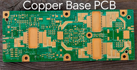
What are Heavy Copper PCBs?
Heavy copper PCBs are generally defined as printed circuit boards that utilize copper weights of at least 3 oz/ft² per layer, significantly more than standard PCB copper thicknesses that are from 0.5 to 3 oz/ft².
Heavy copper PCBs are primarily used to increase current-carrying capacity and enhance thermal management, which is essential for power electronics and other high-demand applications. By increasing copper mass, the board is able to carry high currents with only minimal increases in trace width compared to using lower copper weights.
These boards, also referred to as thick copper PCBs, can be fabricated with copper weights up to 10 oz/ft².
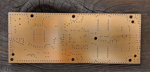
A four-layer PCB with three layers of one-ounce copper with GETEK dielectrics and one of solid 45-oz Cu base.
|
|
Copper Thickness Range |
Applications |
|
Standard PCB |
0.5 oz/ft² (≈17 µm) to 3 oz/ft² (≈105 µm)
|
Low-power or digital applications where current demands and heat dissipation are modest
|
|
Heavy Copper PCB |
4 oz/ft² (≈140 µm) up to 10 oz/ft² (≈700 µm)
|
High-current, high-power electronics requiring robust thermal management
|
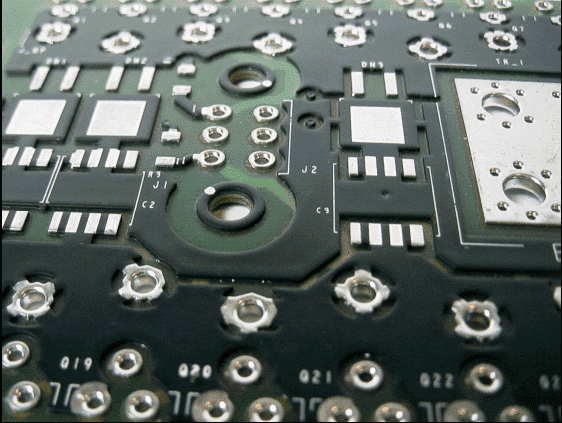
Heavy Copper PCB Construction
Heavy copper PCBs are manufactured using four primary methods, each balancing cost, accuracy, and performance.
1. Thin Base, Full Plating
This high-precision but costly method starts with a very thin copper layer. Heavy copper is built up entirely through plating, then the base layer is etched away. Because this approach often requires 20+ hours of plating, it's reserved for high-performance applications where thicker copper in holes improves current capacity and thermal management. Best for fine-line, high-current designs.
2. Mid-Weight Base, Partial Plating
This common method uses a copper layer about half the final desired thickness. Additional copper is plated, then the full thickness is etched. It offers good cost-efficiency, though resolution is lower than the thin-base method. Plated features are more precise than etched ones, and designers must carefully calculate copper buildup in holes.
3. Thick Base, Minimal Plating
In this budget-friendly option, a thick copper base is lightly plated and etched. It’s the least expensive but offers limited trace resolution and poor current handling in holes. Typically used in low-tech applications where performance demands are minimal.
4. Ultra-Thick Copper
Copper thicknesses from 0.020" to 0.040" can be achieved for high-power applications, like Buss Bar replacements. However, extended plating times lead to surface bumps, and imaging through thick photoresist reduces resolution and edge quality. Despite this, the method allows for very robust conductors and high-current paths.