There are 8 different types of vias used in PCB design. Some are more common than others, with each serving different purposes depending on the board’s layer structure, signal integrity requirements, thermal needs, and density. While classifications can vary slightly depending on context, the primary types of PCB vias include:
Through-Hole Vias: Go through the entire board from top to bottom, connecting all PCB layers.
Blind Vias: Connect the outer layer to one or more inner layers, but don't go all the way through.
Buried Vias: Connect only internal layers and are invisible (thus, buried) from the surface.
Microvias: A very small, laser-drilled via (≤150 µm), used in HDI boards.
Stacked Vias: Multiple vias stacked vertically across high density layers.
Staggered Vias: Vias offset from one another across layers, not stacked directly.
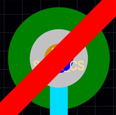
Tented Vias: Vias covered with a solder mask for protection or isolation.
Via-in-Pad (VIP): A via placed directly beneath a component pad, often filled and capped.
A via (technically stands for Vertical Interconnect Access) is a small, drilled hole in a multi-layer printed circuit board (PCB) that allows electrical signals to pass between the layers. Vias serve as vertical connections between the copper traces on different layers, enabling complex routing in compact designs.
Vias are plated with copper to conduct electricity and are filled, tented, or left open depending on their function and placement. The dimensions and structure of a via are carefully calculated, factoring in via aspect ratio, current-carrying capacity, and mechanical stability.
The plating process generally involves electroless copper deposition to create an initial conductive layer, followed by electroplating to build up the desired thickness. Uniform plating is critical for electrical performance, particularly in controlled impedance designs and high-current applications.
At San Francisco Circuits, we specialize in supplying complex bare and assembled circuit boards at prototype and production volumes.
Vias are essential to meeting the demands of today's compact, high-speed, and multilayered electronic designs.
These are the 7 most common vias used in PCB manufacturing, along with our insights into their fabrication and integration into a bareboard.
Blind vias connect an outer layer of the PCB to one or more inner layers without going all the way through the board. This helps free up routing space on inner layers and supports higher-density designs.
They can be fabricated using precision-controlled depth drilling or laser drilling. It's critical to maintain ideal via aspect ratios, ensuring reliability and structural integrity during lamination and thermal cycling.
The most common aspect ratio is 1:1 with the diameter and depth of the laser drilled via being 3 mils. The depth should not exceed the diameter, as deeper holes increase the likelihood of air bubbles becoming trapped at the bottom, which can prevent proper plating and result in an open circuit.
Blind vias are typically used in designs where space is limited, such as in smartphones, medical implants, and RF devices.
Blind via with trace entering bottom layer (layer 6) and exiting mid-layer (layer 3). The hole does not continue all the way to the top layer, allowing the top layer traces to pass through over the hole.
Buried vias connect internal layers without reaching the outer surfaces of the PCB. They are used to maximize routing density while maintaining external layer real estate for components and critical traces.
Buried vias are used in multilayer stackups by laminating sub-assemblies before final lamination. Proper fabrication of buried vias requires meticulous alignment and verification throughout the process.

A buried via with the trace entering mid-layer 1 (layer 3) and exiting mid-layer 2 (layer 4). The hole is not present on layers above layer 3 or below layer 4, allowing traces on all other layers to pass over the top or below the via.
To help plan your multi-layer stackup and blind/buried vias, use our PCB stackup calculator / design tool.
Through-hole vias are the most common type of via. These vias run through the entire board from the top layer to the bottom layer, physically connecting all the layers in between. Because they span the full board thickness, they are relatively easy to manufacture and inspect.
While through-hole vias occupy more board space compared to blind or buried vias, they are often used for their high mechanical strength and reliable electrical performance. This makes them ideal for applications requiring strong structural support, such as connectors, power components, or boards subject to mechanical stress.
Through-hole vias are often used in multilayer PCBs where connectivity across all layers is needed. They can be optimized for specific performance needs using calculations for current-carrying capacity, impedance, and thermal behavior.

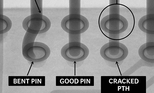
Plated thru hole (left) vs. non-plated thru hole (right)
Microvias are tiny vias that are typically less than 150 microns in diameter and used predominantly in HDI PCBs. They enable extremely fine-pitch BGA routing and are essential in smartphones, wearables, aerospace, and medical applications.
Microvias are built predominantly using UV laser drilling or CO2 laser methods.
It typically penetrates across only two circuit layers unless configured as a stacked/staggered microvia or as a skip via.
While microvias are commonly used in HDI PCBs, traditional mechanically drilled blind and buried vias can also be implemented in multilayer PCB designs as well.
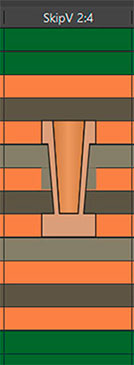
A skip microvia that connects a trace from layer 2 to layer 4. Note that layer 3 cannot be connected with this type of via and is “skipped” all together, optimizing the manufacturing operations and reducing the need for drilling and plating to make an annulus and landing pad on layer 3.
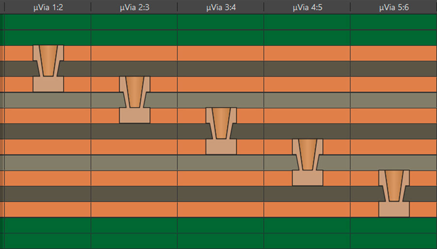
Stacked vias are multiple vias aligned vertically across layers in a multilayer PCB. These structures are typically formed by stacking blind vias or microvias on top of one another, allowing electrical connections through several layers without using a traditional through-hole via. They are essential in high-density interconnect (HDI) boards where space is limited and complex routing is required.
The formation of stacked vias involves sequential lamination, via drilling, plating, and filling steps repeated at each stage. Precise alignment and process control are critical to avoid reliability issues such as stress concentration or poor conductivity. Stacked vias are filled with electroplated copper to ensure robust vertical interconnection and consistent performance.
When a blind via exceeds its allowable aspect ratio, typically around 1:1, stacked microvias are used instead. This helps maintain structural integrity and enables additional layers to be connected without compromising reliability or requiring full-through vias.
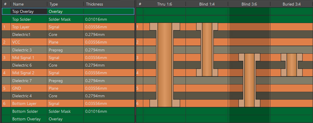
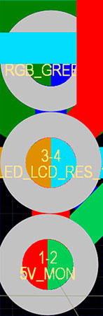
Stackup manager with various via configurations including full-stack thru-hole via, blind via from top layer, blind via from bottom layer, and buried via between mid-layers.
Example of 3 stacked vias. The via on top connects a trace from layer 1 to layer 2, the via in the middle connects traces between layer 3 and layer 4, and the via on the bottom connects a trace from layer 6 to a plane on layer 5.
Staggered vias are similar to stacked vias but are offset layer to layer, reducing the risk of mechanical failure. They are commonly used in designs where reliability under thermal or mechanical stress is critical.
While staggered vias take up slightly more space, they offer better durability and are easier to manufacture than stacked vias in many cases.
Staggered vias typically improve signal quality and can be more complex to design, but their manufacturing cost is typically lower than stacked vias. The cost is typically less as staggered vias on different layers do not overlap, requiring less precision than their stacked counterparts.

Example showcasing the staggered arrangement of the three stacked vias referenced in the previous illustration.
Layer stack manager showing several buried and blind microvia configurations that can be used for stacking and staggering.
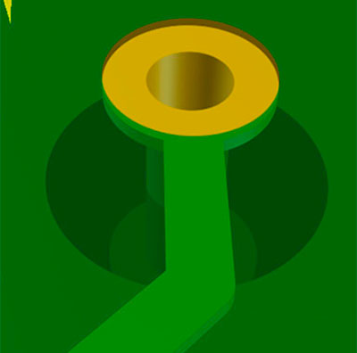
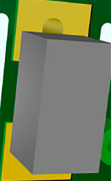
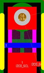
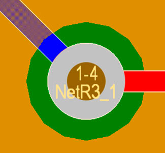
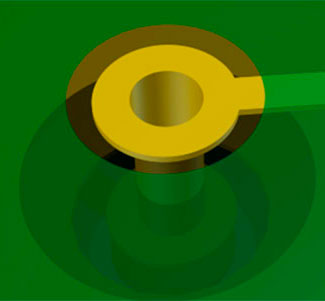
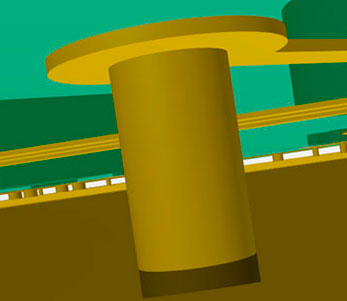
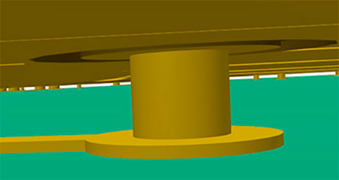
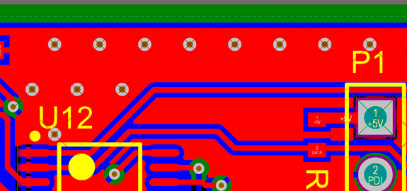
Via-in-pad (VIP) refers to the placement of a via directly beneath a component pad, a technique commonly used under ball grid array (BGA) packages and other high-density components. This design minimizes routing space and shortens signal paths, making it ideal for compact layouts.
The via is typically plated, filled with conductive or non-conductive epoxy, then planarized and capped plated to create a smooth, solderable surface. This process helps prevent solder from wicking into the via during assembly, which could otherwise cause poor solder joints or open connections.
Via-in-pad construction requires tight manufacturing tolerances and is a key method for achieving miniaturized and high-performance designs. These challenges become significantly more complex in double-sided BGA assembly, where vias, pads, and solder joints must be controlled on both sides of the PCB.
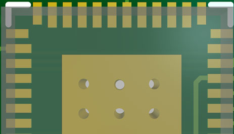
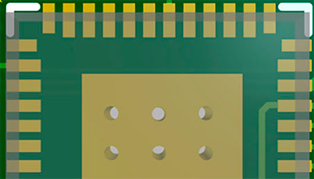
A footprint with a thermal pad that includes an array of via-in-pad thermal reliefs. This is common for thermal pads to help with thermal dissipation and expanding the amount of copper to other layers to help with heat-sinking. The other example to the right indicates a simple passive component (like a resistor) that contains a via in one of its pads.
Tented vias are covered with solder mask to prevent contamination, aid in reducing the risk of solder wicking during assembly, and protect against short circuits. This technique enhances the reliability of the board and improves the integrity of the solder mask, particularly in dense layouts.
Tenting is commonly applied to vias located close to component pads or underneath components, where exposed copper could interfere with soldering or assembly.
Depending on design requirements, vias may be partially or fully tented, following IPC-4761 guidelines for solder mask coverage.
Read more: Via Tenting Principles

Examples of PTH vias tented and untented. The trace is entering the top layer and exiting from the bottom layer.
Thermal vias are used to transfer heat away from high-temperature components such as power ICs, voltage regulators, or LEDs. These vias are typically placed beneath thermal pads and connect to internal copper planes or external heat sinks to help dissipate excess heat throughout the PCB.
Arrays of thermal vias are often arranged to maximize conductivity, with considerations for via spacing and plating thickness. Effective use of thermal vias is essential in designs requiring reliable thermal management, such as power electronics and high-brightness LED systems.
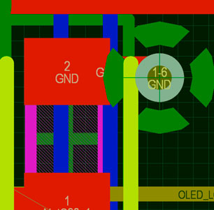
Thermal vias can be designed with thermal reliefs to mitigate solderability issues (common for small passive components) or configured as direct-connect for optimal heat dissipation. They are frequently incorporated as via-in-pad structures within the thermal pad or high-current path of the component's PCB footprint. These are shown in the images below (direct connect in a thermal pad on the left, thermal relief for a passive component via ground connection on the right).
Depending on the design needs, vias may be tented (covered with solder mask) or left exposed.
Via tenting involves covering the via opening with solder mask to protect it from contamination, solder wicking, or electrical shorts. Masking, more broadly, refers to the selective application of solder mask to expose or protect different parts of the PCB, including vias. In the context of vias, tenting is one form of masking, while others include plugging (filling the via), capping (adding a layer over it), or leaving the via completely exposed. The choice between these options depends on the PCB’s assembly method, whether solder paste will be applied over the vias, and whether cleaning or inspection access is needed. IPC-4761 outlines the standardized classifications for these methods.
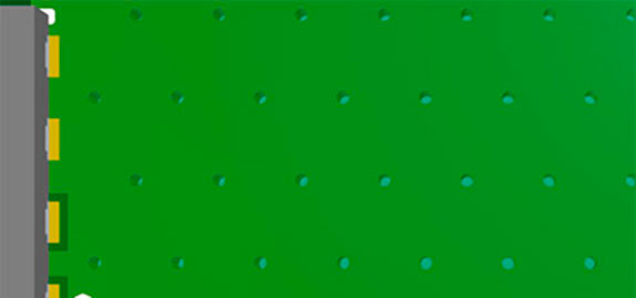
Via stitching refers to the practice of placing multiple vias along a ground or power trace to improve thermal dissipation, grounding for signal performance, or EMI shielding. This is commonly used in RF designs and multilayer ground planes.
We specialize in all printed circuit boards including flex PCB, metal core PCB and military PCBs. Our fabrication and assembly capabilities push our circuit board technologies further than standard boardhouses with much higher wiring densities and finer lines and spaces.
San Francisco Circuits is your single source solution for PCB manufacturing and assembly.
Whether you’re working on a prototype with blind vias and thermal via arrays or a production run of flex circuit boards, we have the experience and resources to deliver.
Let us help you manufacture it right the first time.
PCB School
Standards like MIL-PRF-55110, MIL-PRF-50884, and MIL-PRF-31032 exist to enforce reliability, traceability, and performance in environments where failure isn't acceptable.
PCB School
Flying probe testing has been the golden standard of functional testing for low volume, prototype runs since the late 80s and 90s. It effectively flips the approach of the traditional in-circuit (ICT) bed-of-nails fixture test, where a custom-built frame with hundreds of spring-loaded pins contact test points simultaneously.
PCB School
Double-sided Ball Grid Array (BGA) assembly maximizes component density without increasing board size, enabling high-performance designs for applications ranging from smartphones and IoT devices to medical and industrial electronics.
PCB School
Managing strain during press-fit connector insertion is essential for high-density PCB reliability. Discover best practices and how San Francisco Circuits ensures reliable assembly for HDI, mil-spec, and medical applications.

PCB School
Discover why NIST 800-171 compliance is essential for PCB manufacturers. As a PCB buyer, learn how this cybersecurity framework safeguards your sensitive data & ensure you are engaged with a boardhouse that meets these requirements.
PCB School
San Francisco Circuits covers board-level tips for the design & layout of high-speed circuits in advanced applications.
