The predominant method used for attaching surface mount components to printed circuit boards during PCB assembly is reflow soldering.
Reflow soldering is a four-step process that involves:
Preceding the reflow soldering process, a stencil is created and used to apply the solder paste to the contact pads on the PCB. A pick-and-place machine then places the components on the board. For double-sided boards, the board is flipped and the process is repeated.
The board then goes into the reflow oven to form the solder joints and bind the components to the board.
The initial heating step is to ensure the assembly and solder reach a specified temperature at a specific rate, also known as ramp rate. The heating rate during this step is defined by the solder paste’s datasheet and guidelines but usually is 2ºC/second or less.
Heating the solder too quickly can cause splattering, leading to solder balls/beads. Solder beading will fail minimum gap requirements, affecting the board’s electrical reliability. Components can also be damaged if heating guidelines are not properly followed during these steps.

Solder beading, pictured above, is just one of several issues that can arise from excessive heating & poor SMT reflow profile.
Image Source: National Physics Laboratory Soldering Defects Database
The thermal soak step lasts just 1 to 2 minutes and will get all the components to the exact required temperature for reflow in step 3. It’s important to note that the initial heating step is critical prior to the soak step to ensure the heating rate is sufficiently gradual. Likewise, it’s critical the soak phase is done at the perfect temperature or the flux (flowing agent in the solder paste) can suffer from defects like graping and/or head-in-pillow (HIP or HNP).
The reflow step brings the oven, board, components, and solder to the maximum temperature during the entire process. In this step, the solder paste is melted to fuse the solder joint. The solder flux activates and the powder melts, forming the joint, while the flux evaporates away.
It is critical that the maximum temperature is established properly during the reflow profile definition. This maximum should be below the component that has the lowest maximum temperature allowance, but above the reflow melting point of the solder paste used. This maximum temperature is a delicate point that needs to be quite precise - it can not be too hot (to avoid thermal damage to board and/or components) or too cool (to avoid poor coalescence / solder joints).
“Time above liquidus” (TAL) is also established - the length the solder is held above its melting point. This time is critical to ensure appropriate “wetting” materializes between the components and board. This time is typically 30 seconds to 1 minute. Too much time at this temperature can cause damage to the components or can lead to brittle solder joints.
At the melting point, the flux within the solder paste reduces surface tension at the juncture point of the metals to achieve metallurgical bonding. At this point, the solder powder spheres combine with the board and components.
Macro View of LED component mount by reflow soldering
A reflow environment with nitrogen is often recommended or required by assembly specifications to reduce surface oxidation. Oxygenated reflow environments are often not compatible with the flux in solder paste, leading to non-solderable oxidized surfaces and wettability issues. Many soldering defects can arise from oxidation, like the head-in-pillow defect.
An oxygen-free environment, with the use of nitrogen reflow soldering, will prevent or drastically slow down oxidation, improving wettability, to reduce these types of defects.
During the reflow process, the chamber of the oven is filled with nitrogen, forcing the oxygen to the bottom of the chamber and reducing its exposure with the solder paste.
Nitrogen reflow soldering, however, does have some negatives including high cost and some other potential effects like increased tombstone phenomenon and solder wicking / solder drainage.
The final step is to simply cool the reflowed board at a controlled rate. It is important to cool it at a governed rate, typically 2 to 4°C per second, to properly solidify the solder joints, while avoiding thermal shock. Generally, a faster rate will result in a finer grain structure in the metals, minimized intermetallic growth, and stronger solder joints, but too fast can result in thermal shock. Note that a max of 6°C per second is often specified for boards but this rate does offer significant shock risk to the assembly.
This step is also challenging as the cooling rate is not easily controlled. Some reflow ovens have the capability to control the cooling rate by varying a cooling fan. Other variables also come into effect, such as ambient air temperature and the thermal mass of the board (higher thermal mass will cool more slowly).
It’s critical for all parties involved (design, engineering, and technicians/operators of the oven) to establish the proper SMT oven reflow profile/thermal requirements of the PCB & components to avoid damage from overheating.
In addition to temperature requirements, reflow technicians / NPI engineers must establish the line speed, process speed, and oven heated length. These requirements are critical to ensure a defect-free assembly in addition to a smooth PCBA workflow, keeping surface mount assembly in lockstep with PCB fabrication rate for production-level orders.
All of these reflow parameters help to build an acceptable reflow profile that guides the selection of which reflow oven to use by the PCBA / SMT assembly shop.
The reflow soldering profile considers:
A reflow profile is tested by running a sample assembly with thermocouples on various board locations to measure the temperature changes across the test PCB as it runs through the oven. The goal is to create a profile that is hot enough to melt the solder to form successful solder joints without causing damage to the board and its components.
The commercial-level reflow soldering process is done in a reflow oven that contains a conveyor belt that moves the PCB being assembled through various heat zones. These ovens can be infrared, convection, or combination infrared-convection. Most production-level assemblies will use a conveyor type convection oven that supports the boards along its edges to allow for double-sided soldering. The double-sided board assembly process may also involve supporting the boards along their centers to avoid sagging during high heat stages.
Some ovens come with automated control of support widths for complex size changes and multiple board assemblies. Other machines have specialized convection fans and closed loop systems for ultra-controlled environments.
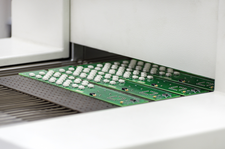
Assembled PCBs Exiting Reflow Oven
In an infrared oven, the heat source is a ceramic infrared heater, which heats the oven by means of radiation.
Convection ovens, on the other hand, heat the air within the oven using convection and conduction.
Board requirements may call for an oxygen-free atmosphere to minimize oxidation; these ovens reflow PCBs using nitrogen.
A fourth heating method is also available via vapor phase soldering ovens, where a liquid is used for thermal energy transfer. Vapor phase soldering is energy-efficient, low-risk for overheating, and inherently oxygen-free.
Reflow soldering can be used for plated through-hole components (called intrusive soldering), although wave soldering is typically the preferred method for attaching these components. Most commonly, reflow soldering will be used for boards that use a mix of SMT and PTH components in an effort to reduce assembly costs (by eliminating the wave soldering requirement). However, it is not always recommended and must be consulted on by experienced technicians. Certain specialized PTH components may even require hand soldering.