Press fit connectors are common in high-density PCB designs - powering 5G infrastructure, electric vehicles, aerospace systems, and advanced medical devices. Their ability to deliver high I/O counts without the heat risks of soldering makes them indispensable for modern electronics.
But here’s a hidden risk: If strain during insertion isn’t properly managed, it can lead to latent solder joint cracks, fractured plated through holes (PTHs), or deformed pins. These failures often escape detection during testing and only surface in the field - causing warranty returns, costly recalls, or even mission-critical system outages.
In this post, we’ll cover how stress impacts PCB reliability, safety thresholds, and how to overcome these challenges in your application.
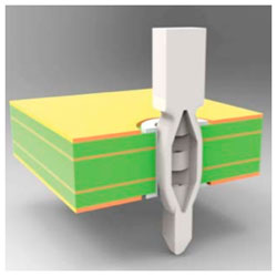
Press fit technology uses an interference fit, where connector pins are pressed into PTHs with near-zero clearance to form a tight mechanical and electrical bond. A controlled force (up to 600 lbs for a 60-pin connector) drives this process, causing the PCB to flex. This flexure generates strain that can crack solder joints, PTH barrels, or deform pins, threatening reliability in high-stakes applications like aerospace or medical devices.
For instance, a medical client could face costly MRI control board failures due to BGA cracks near press fit sites, underscoring the need for precise strain management.
There are two main types of press-fit pins:
Both types of press-fits can either be soldered or solderless, depending on the application (pin count/density, risk of thermal stress during soldering, simplicity of assembly).
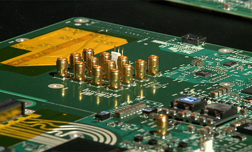
Press-fit pins are commonly used by many connector manufacturers and greatly improve system reliability and performance. The pin is a stamped metallic spring section sized slightly larger than the finished hole. During insertion it elastically deforms and creates continuous radial force against the PTH barrel, providing low contact resistance and mechanical stability.
The picture below shows a multispring press-fit pin from TE (picture taken from this whitepaper).
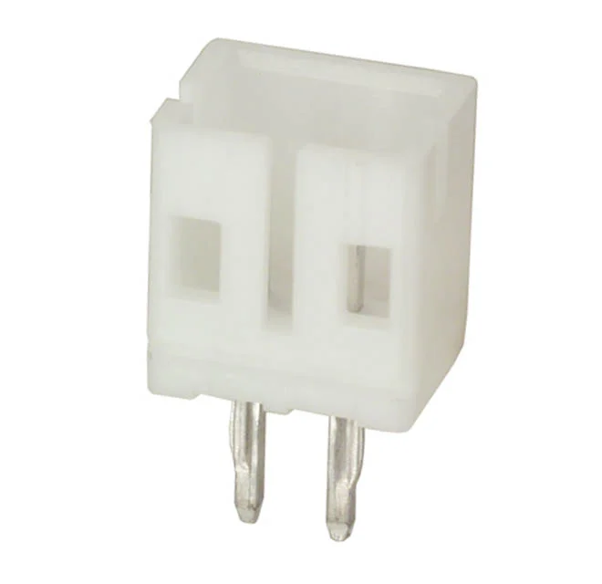
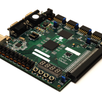
This press-fit pin can be applied both in low-density and high-density applications. The pictures below show very common connectors with press-fit pins that help provide mechanical support and low-resistance. Solder would typically be applied to this kind of connection.
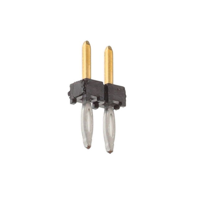
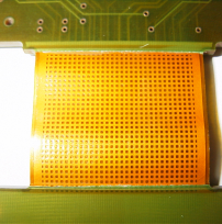
For higher density pin arrays (like the examples shown below), the connector can be inserted without the need for solder (picture taken from this whitepaper) but may require a sophisticated tool for managing its insertion properly.
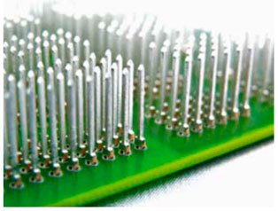
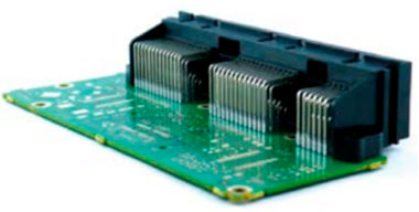
Image source: TE
Though widely used, errors anywhere in the press-fit system (incorrect hole, uneven plating, contamination, incorrect insertion force) can produce latent defects that can survive visual inspection but fail under thermal cycling or vibration.
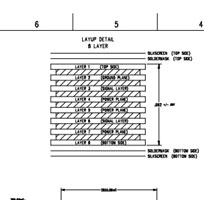
As 5G, automotive, and aerospace applications demand higher signal speeds and pin counts, press fit connectors are critical. Unmanaged strain can cause solder joint cracks, PTH barrel fractures, or pin deformation, leading to open circuits or latent failures. Strain decreases with distance, but factors like PCB thickness, asymmetric stack-ups (e.g., HDI, rigid-flex), or exotic laminates (e.g., metal core) amplify risks. For example, metal-core PCBs, common in high-heat applications, may require thicker fixtures to control flexure.
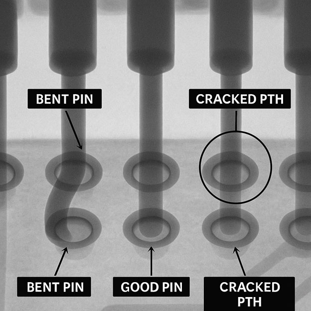
X-ray inspection reveals hidden defects such as bent pins and cracked PTH barrels in press fit assemblies.
Press-fit PCBA connectors are powerful enablers of high reliability, solderless and solderable interconnects when the entire press-fit system (connector design, PCB hole/plating quality, insertion tooling, inspection, and qualification) is treated as a single engineered solution.
Following OEM specs, using controlled insertion and inspection, avoiding counterproductive repairs, and incorporating an inspection and validation process are the practical steps that result in a high-reliability press-fit system.
.png)
San Francisco Circuits specializes in getting complex, high-end PCBs built fast, including flex, rigid-flex, metal core, and mil-spec.
We run by a simple motto with complex meaning: Bridging Concepts with Reality. Our specialty is the single-source supply of both bareboard and assembled PCBs, from standard builds to the most advanced technologies.
Many of our customers bring us designs that typical boardhouses can’t manufacture or assemble. We welcome that challenge. Whether it’s prototype or production, our expertise ensures high-quality multilayered PCBs delivered on time, even when requirements push beyond industry norms.

PCB School
Standards like MIL-PRF-55110, MIL-PRF-50884, and MIL-PRF-31032 exist to enforce reliability, traceability, and performance in environments where failure isn't acceptable.
PCB School
Flying probe testing has been the golden standard of functional testing for low volume, prototype runs since the late 80s and 90s. It effectively flips the approach of the traditional in-circuit (ICT) bed-of-nails fixture test, where a custom-built frame with hundreds of spring-loaded pins contact test points simultaneously.
PCB School
Double-sided Ball Grid Array (BGA) assembly maximizes component density without increasing board size, enabling high-performance designs for applications ranging from smartphones and IoT devices to medical and industrial electronics.

PCB School
San Francisco Circuits covers the 8 types of PCB vias including blind, buried, microvias, through-hole, stacked, & thermal vias - what they are, how they work, & where they’re used in advanced PCB design.

PCB School
Discover why NIST 800-171 compliance is essential for PCB manufacturers. As a PCB buyer, learn how this cybersecurity framework safeguards your sensitive data & ensure you are engaged with a boardhouse that meets these requirements.
PCB School
San Francisco Circuits covers board-level tips for the design & layout of high-speed circuits in advanced applications.