Single-Source Printed Circuit Fabrication & Assembly - Standard & Advanced Technologies
Email us for a PCB quote
or call us at 1-800-SFC-5143




San Francisco Circuits runs by a simple motto with complex meaning
Our specialty is single-source supply of bareboard and assembled PCBs. Whether it's standard technologies, or complex, advanced technologies, with us you receive unparalleled technical expertise with some of the most progressive solutions available.
We are capable of standard and advanced technology prototype and production runs, delivering high quality multi-layered PCBs from elaborate layouts on time.
Many of our customers request PCB production that is outside the capabilities of normal circuit board providers. Do you have an intricate concept that typical boardhouses can't manufacture or assemble? We welcome that challenge and will turn your designs into reality.
ISO 9001-2015 CERTIFIED
Explore our full list of PCB production capabilities
Our expertise in circuit boards is not limited to PCB manufacturing, but extends to PCB assembly.
Our highly skilled engineers will partner with you to achieve economical perfection in your multi-layered layout – anything from a basic double-sided bareboard to intricate rigid flex PCB applications.
We strive for our customers to feel that our service is so unique and valuable that they would want to work with us forever.
We understand that you want solutions - you want what you need and not what a boardhouse wants to sell you. Through a diverse portfolio of vendor relationships, our board technology capabilities ensure you will receive a final deliverable that meets the stringent specifications you require.
We specialize in all printed circuit boards including flex PCB, metal core PCB and military PCBs. Our fabrication and assembly capabilities push our circuit board technologies further than standard boardhouses with much higher wiring densities and finer lines and spaces.
San Francisco Circuits is your single source solution for PCB manufacturing and assembly.
View our full offering of PCB production capabilities and register today for an instant PCB quote from our online quoting system. Our experts are available to consult you on your PCB fabrication project via phone, email or live chat.
From manufacturing to circuit assembly, SFC can source it all.
PCB School
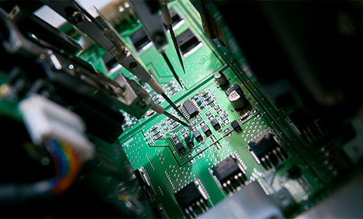
Flying probe testing has been the golden standard of functional testing for low volume, prototype runs since the late 80s and 90s. It effectively flips the approach of the traditional in-circuit (ICT) bed-of-nails fixture test, where a custom-built frame with hundreds of spring-loaded pins contact test points simultaneously.
Capabilities
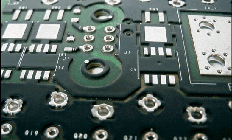
San Francisco Circuits is an industry-leader in heavy copper PCBs. Up to 10oz/ft², we can turn your copper core PCB order as fast as 72 hours with expert precision. Made in USA.
PCB School
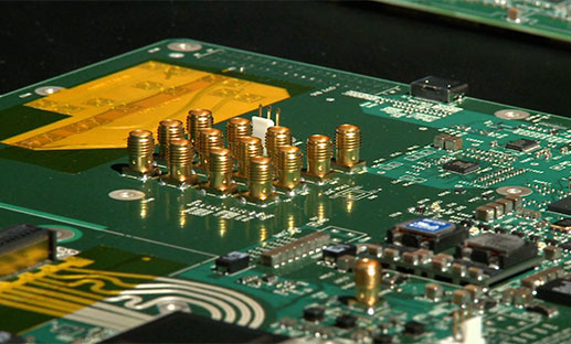
Double-sided Ball Grid Array (BGA) assembly maximizes component density without increasing board size, enabling high-performance designs for applications ranging from smartphones and IoT devices to medical and industrial electronics.
