In the realm of printed circuit board (PCB) manufacturing and assembly, attention to detail is paramount. Every element, from component placement to orientation, plays a crucial role in ensuring a successful and efficient assembly process. One vital aspect of this process is the proper utilization of the assembly drawings; in particular, the significance of polarities, Pin1 marking, and anode/cathode markings.
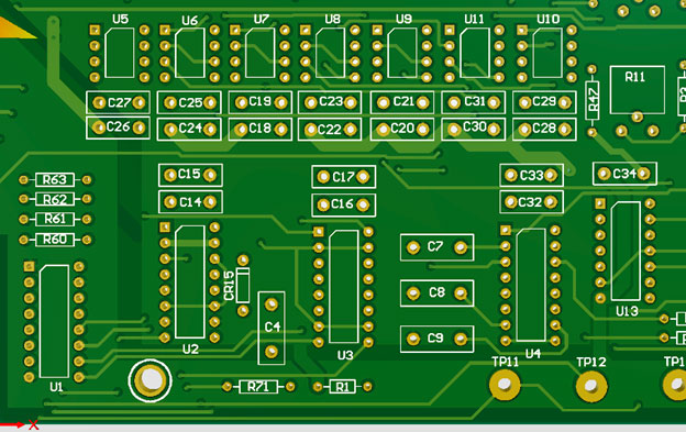
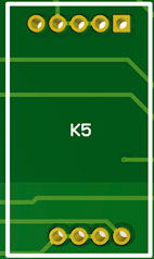
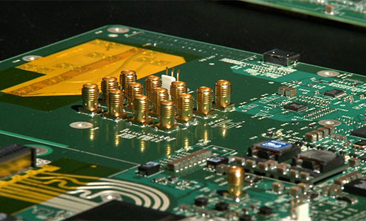
Example of several through-hole components mounted in the same direction to optimize wave soldering profile.
Understanding the XY File and Component Locations
The XY file, also known as the pick and place file, serves as a fundamental reference for component locations on the PCB. It provides the X and Y coordinates for each component, along with rotations, facilitating accurate placement during assembly.
The Role of Rotations and Component Orientations
While standards exist for component rotations, such as counterclockwise/clockwise, 0, 90, 180, or 270 degrees, exceptions and software settings can influence this aspect. The orientation of the PCB itself, when fed into the assembly machine, can impact the rotation requirements for specific components. Additionally, when a PCB manufacturing facility creates a multi-up board panel to assemble multiple boards simultaneously, the fabrication files may alter the way component orientations are viewed at assembly. Sometimes it is necessary to have the boards orientated 180 degrees from each other.
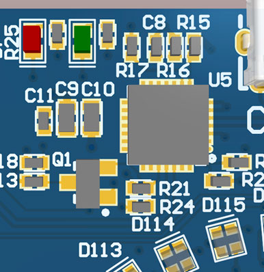
The red and green LED cathodes are indicated with silkscreen bars on bottom. The Pin1 orientation of the IC is found in the bottom right of its footprint. Cathode indications of several dual LEDs (D113, D114, D115) annotated again with silkscreen bars.
Importance of Polarities (Anode and Cathode Markings)
Polarities play a vital role in ensuring the correct functioning of electronic components on a PCB. These components are polarized with an anode and cathode pin. PCB assembly drawings often include markings or symbols that indicate the polarity of these components, diode symbols and physical indicators, either as text annotations or silkscreen markings or both.
By adding polarities to the silkscreen, assembly technicians can avoid improper connections and potential damage to the components.
Polarized components can only be connected in one specific direction. These components may have a variable number of pins, ranging from two to hundreds, with each pin serving a distinct function and/or position.
Non-polarized components, on the other hand, can be connected in any direction without affecting their performance.
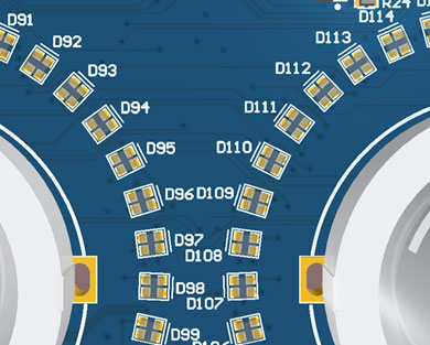
Note the orientations of all of the dual LEDs shown in a circular pattern. These are non-standard orientations that would be accounted for in pick and place files.
Examples of polarized components include batteries, power supplies, diodes, electrolytic capacitors, LEDs, transistors, MOSFETs, and voltage regulators.
When it comes to power supply connections, batteries and power supplies have distinct positive and negative terminals, usually marked with symbols or colors.
Transistors, MOSFETs, and voltage regulators are three-terminal components that come in various package types. Their pin configurations can be determined by referring to their respective datasheets and matching them with the package's physical features.
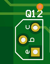
Example of a through-hole transistor and respective pins; Pin1 is indicated with a square pad.
Example of a thru-hole power supply with its pins detailed in silkscreen.
Even seemingly non-polarized components like resistors can have polarized variants, such as resistor arrays, where the common connection makes the overall array non-symmetric.
Manufacturers incorporate various indicators to aid in identifying component polarity. These indicators vary based on the type of component:
Diodes often feature a stripe or band near their cathode terminal, denoting their polarity. Additionally, diode symbols on the PCB layout and datasheets also assist in proper orientation.
The negative terminal of electrolytic capacitors is typically marked with a negative symbol ("-") or colored stripe. Longer positive leads can further assist in correct placement.
LEDs have longer and shorter leads, with the longer lead being the positive anode. The flat edge of the LED casing also points to the negative cathode.
Paying attention to markings, symbols, and datasheets ensures the accurate placement and orientation of components, minimizing the risk of damage or malfunction. It’s crucial to accurately represent polarities in assembly drawings to maintain design integrity.
Example of a 2-pin battery connector with Pin1 marked with a dot and a square pad.
Non-Polarized Components
Examples of non-polarized components include resistors, capacitors, and inductors, although there may be exceptions. Capacitors, in particular, can be non-polarized (such as small ceramic capacitors) or polarized (like electrolytic and tantalum capacitors), with clear markings indicating their polarity.
Pin1 Marking / Zero Orientation
Pin1 marking is another crucial element. The term "zero-orientation" of a component denotes the position of Pin1. It refers to the identification of the first pin or lead of a component.
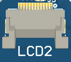
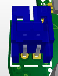
Example of a Pin1 marking for a flex connector going to an LCD.
Proper marking of pin1 aids in the correct alignment of the component during assembly. By aligning pin1 with the corresponding marking on the PCB, technicians ensure the accurate placement of the component, preventing any misalignments that could hinder functionality. There exist two distinct standards governing this rotation, based on IPC’s guidelines. The first is known as "Level A Zero Component Orientation," where pin1 is situated in the upper-leftmost corner of the package when rotation is zero. In 2009, a subcommittee of the IEC introduced a redefined zero orientation called "Level B," which specifies that pin1 should be in the lower-leftmost corner when rotation is zero.
Most standard library component footprints predominantly employ the Level A zero orientation. This familiarity makes it the preferred choice for the majority of PCB designers. In fact, many designers gravitate toward the Level A orientation without necessarily recognizing it, and some might not even be aware of the concept of zero orientation in general.
Some typical best practices can be implemented during design/layout to ensure optimal placements and reduce errors during reflow:
Example of through-hole diodes and their cathode (negative) silkscreen markings on the left side of the footprint.
Example of a quad relay component; its Pin1 is indicated with a square pad. This is commonly done for through-hole parts.
In some instances, components are grouped to optimize common pin connections to a power bus. If altering their orientation isn't feasible, connecting these components to the power bus via thinner traces prevents issues like tombstoning during solder reflow.
Further consideration pertains to components placed at the edge of the board. During separation from manufacturing panels, factors like part positioning and orientation must allow space for scoring tools to prevent defects or component damage.
Learn more about PCB reflow soldering here.
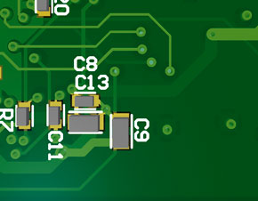
Cluster of capacitors supporting a regulator on the opposite side. Positions have been optimized for best decoupling performance over reflow profile.
Precise and accurate PCB assembly drawings are critical for a successful manufacturing and assembly process. Paying close attention to these details ensures that components are correctly assembled, reducing the risk of errors or failures.
By adhering to industry standards and leveraging advanced software tools, designers, manufacturers, and assembly providers can enhance the efficiency and reliability of their PCB assembly processes.
PCB School
Standards like MIL-PRF-55110, MIL-PRF-50884, and MIL-PRF-31032 exist to enforce reliability, traceability, and performance in environments where failure isn't acceptable.
PCB School
Flying probe testing has been the golden standard of functional testing for low volume, prototype runs since the late 80s and 90s. It effectively flips the approach of the traditional in-circuit (ICT) bed-of-nails fixture test, where a custom-built frame with hundreds of spring-loaded pins contact test points simultaneously.
PCB School
Double-sided Ball Grid Array (BGA) assembly maximizes component density without increasing board size, enabling high-performance designs for applications ranging from smartphones and IoT devices to medical and industrial electronics.
PCB School
Managing strain during press-fit connector insertion is essential for high-density PCB reliability. Discover best practices and how San Francisco Circuits ensures reliable assembly for HDI, mil-spec, and medical applications.

PCB School
San Francisco Circuits covers the 8 types of PCB vias including blind, buried, microvias, through-hole, stacked, & thermal vias - what they are, how they work, & where they’re used in advanced PCB design.

PCB School
Discover why NIST 800-171 compliance is essential for PCB manufacturers. As a PCB buyer, learn how this cybersecurity framework safeguards your sensitive data & ensure you are engaged with a boardhouse that meets these requirements.
