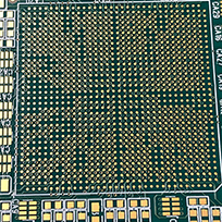
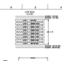
When designing a printed circuit board, one of the first decisions is choosing the appropriate IPC class. Specifying IPC Class 2 or Class 3 affects far more than a PCB's inspection criteria. The class chosen influences how the board is designed, fabricated, tested, and accepted throughout the manufacturing process. It also has a direct impact on cost, lead time, and the number of fabricators capable of producing the board.
The difference isn't how the boards are built. It's how much variation the standard allows during manufacturing and inspection.
That doesn't mean one class is inherently better than the other. The right choice depends on how the finished application will be used. IPC classifications are intended to match manufacturing requirements to the reliability demands of the end product. A higher class doesn't necessarily produce a better PCB. It produces a PCB built to satisfy more stringent reliability and workmanship requirements for applications where failure is unacceptable.
IPC stands for Institute of Printed Circuits and is the global trade association that develops the industry standards used to design, manufacture, assemble, and inspect printed circuit boards.
As of June 2025, the IPC now is officially named the Global Electronics Association although it is still commonly referred to by the acronym IPC after 70 years of previous use.
Among the standards they maintain are product classification systems that establish the level of workmanship and reliability expected for different types of electronic products.
Rather than ranking boards from "good" to "better," IPC classes match manufacturing requirements to the demands of the application.
IPC-6012 defines three product classes:

Consumer products where basic functionality is the primary requirement and long service life isn't critical.
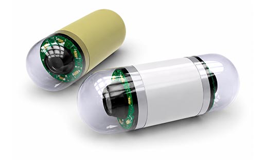
Products expected to provide reliable, continuous performance throughout their intended service life.

Products where continued performance is essential because failure could have significant operational, financial, or safety consequences.
Most commercial PCB projects fall into either Class 2 or Class 3 and those will be the ones we focus on.
Class 2 is the standard used for most commercial and industrial electronics because it delivers dependable performance without the additional manufacturing requirements associated with Class 3.
These products are expected to operate reliably throughout their service life, although occasional maintenance or repair may be acceptable depending on the application.
Common Class 2 applications include:
Class 2 boards maintain high manufacturing quality while allowing limited process variations that don't affect electrical performance or long-term reliability.
For example, IPC-6012 requires a minimum plated through-hole copper thickness of 20 μm (0.787 mil) for Class 2 boards. Internal-layer annular ring breakout is also permitted in certain situations, provided the electrical connection remains intact. These allowances give manufacturers more flexibility while still producing boards that meet the reliability requirements of most commercial applications.
For many products, Class 2 provides the right balance of performance, manufacturability, and cost.
Class 3 is intended for products where continued operation is critical and failure cannot be tolerated. These products often operate in harsh environments, experience extended service lives, or perform mission-critical functions.
Class 3 introduces tighter manufacturing tolerances, stricter acceptance criteria, additional inspection requirements, and enhanced process controls designed to maximize long-term reliability.
Typical Class 3 applications include:
Under IPC-6012, the minimum plated through-hole copper thickness increases to 25 μm (0.984 mil). Annular ring requirements also become more stringent, with far less tolerance for breakout. IPC Class 3 also places tighter limits on board bow and twist to reduce the risk of assembly issues and long-term mechanical stress on solder joints.
These additional requirements increase manufacturing effort, but they also provide greater confidence that the PCB will continue performing reliably throughout its intended service life.
Read more about our MilSpec PCB capabilities and Military Grade PCB Specifications.
.png)
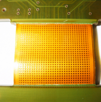
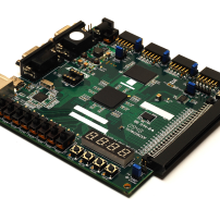
Although both classes use many of the same fabrication processes, they aren't manufactured to the same acceptance standards.
Class 3 places tighter controls on manufacturing and inspection throughout production.
Depending on the design, specifying Class 3 may require longer copper plating cycles, tighter drill registration, enhanced contamination control, additional in-process inspections, and stricter workmanship standards throughout production. These process adjustments improve the board's ability to withstand thermal cycling, vibration, and long service lives, but they also increase manufacturing time and cost.
The impact isn't limited to the fabricator. PCB designers may also need to account for Class 3 requirements during layout. Dense via fields, small annular rings, asymmetric stackups, or marginal design tolerances that satisfy Class 2 may require modification to ensure the finished board can consistently meet Class 3 acceptance criteria.
For that reason, selecting an IPC class should be considered an engineering decision rather than a procurement decision. Choosing the appropriate classification early in the design process helps ensure the PCB can be manufactured efficiently while meeting the reliability requirements of its intended application.
Some of the most significant differences involve plated through holes, annular rings, solder workmanship, and quality verification.
| Category | IPC Class 2 | IPC Class 3 |
|---|---|---|
| Intended use | Dedicated service electronics | High-reliability, mission-critical electronics |
| Reliability expectation | Long service life; occasional interruptions acceptable | Continuous operation; minimal tolerance for failure |
| Minimum PTH plating thickness | 20 μm (0.787 mil) | 25 μm (0.984 mil) |
| Copper void allowance | Up to one void in 5% of holes | No voids permitted |
| Minimum annular ring | Less restrictive; controlled breakout allowed | 1 mil internal, 2 mil external minimum |
| Cleanliness | Standard contamination limits | More stringent ionic and residue limits |
| Workmanship | Commercial quality | Highest workmanship standards |
| Inspection | Standard IPC acceptance | Enhanced inspection, including microsection sampling |
| Manufacturing cost | Lower | Typically 20% to 50% higher, depending on complexity |
| Typical applications | Commercial, industrial, telecom, networking | Aerospace, defense, life-support medical, transportation |
| Barrel fill (assembly) | 75% minimum, with a 50% exception path for qualifying components | 75% minimum, no exception |
One of the most significant differences between Class 2 and Class 3 is the required copper plating inside plated through holes. Class 2 sets a minimum of 0.787 mil average of plating in the hole; Class 3 raises that floor to 0.984 mil.
During fabrication, drilled holes are chemically plated with copper to create reliable electrical connections between PCB layers. Every thermal cycle causes the copper barrel to expand and contract. Over thousands of cycles, thin plating becomes more susceptible to fatigue cracking, especially in high-layer-count boards or products exposed to frequent temperature changes.
The additional copper improves mechanical strength, resistance to thermal fatigue, via reliability during repeated thermal cycling, and long-term electrical continuity. While the difference between 20 μm and 25 μm looks small on paper, it influences multiple fabrication processes. Longer plating times, tighter process control, and additional inspection contribute to the higher manufacturing cost associated with Class 3.
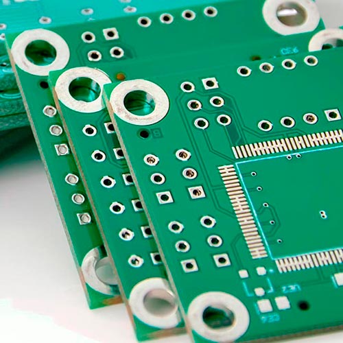
Plated thru holes of varying sizes on a Class 2 board.
Plated through holes create the electrical connections between PCB layers and are among the most critical features affecting long-term reliability. The copper thickness alone doesn't determine reliability. The quality of the drilled and plated hole, including voids, cracks, resin recession, and plating uniformity, also affects long-term performance.
Class 2 tolerates a limited amount of plating voiding, up to one void in 5% of holes. Class 3 does not permit voids at all. Fabricators must maintain stricter process control to minimize defects such as plating voids, barrel cracks, thin copper deposits, poor wall coverage, and incomplete plating.
Many of these defects may not immediately cause electrical failure. Instead, they reduce the safety margin of the interconnection, increasing the likelihood of fatigue failures years later under thermal cycling or vibration. For commercial products, Class 2 acceptance criteria generally provide more than adequate reliability. For systems expected to operate continuously for decades, or where repair is impractical, Class 3 offers additional protection against long-term degradation.
Barrel fill requirements at assembly follow a similar pattern. Both classes require a minimum of 75% barrel fill, but Class 2 allows a 50% fill exception for certain plated through-hole components, provided the lead is visible and surrounding holes meet solder requirements. Class 3 does not carry that exception.
Increasing the minimum copper thickness from 20 μm, the Class 2 specification, to 25 μm for Class 3 improves resistance to thermal cycling, vibration, and mechanical stress. While the difference appears small, it can make a meaningful contribution in applications exposed to demanding operating conditions over many years.
Read more about plated through holes and other PCB via types.

Plated thru hole (left) vs. non-plated thru hole (right)
The annular ring is the copper surrounding a drilled hole. Although it appears to be a small design feature, it plays a critical role in ensuring reliable electrical connections between PCB layers.
During fabrication, drilled holes are rarely perfectly centered. Normal manufacturing tolerances introduce slight drill wander and layer registration variation. If the annular ring is too small, these variations can reduce the amount of copper surrounding the hole, or eliminate it altogether, creating weak electrical or mechanical connections.
Class 2 permits a 90-degree breakout of the hole from the land, provided minimum lateral spacing is maintained. Class 3 does not accept lifted or fractured annular rings, and sets a hard floor: the minimum internal annular ring cannot be less than 1 mil, and the minimum external annular ring cannot be less than 2 mil, measured from the inside of the plated through-hole barrel to the edge of the land. A 20% reduction of that minimum is allowed only in isolated areas caused by defects such as pits, nicks, or dents.
These tighter requirements often translate into more conservative design rules. Vias that comfortably satisfy Class 2 requirements may require larger pads or additional design margin to consistently meet Class 3 acceptance criteria.
A commonly used land-size calculation based on IPC-2221 accounts for the hole diameter, minimum annular ring, and a fabrication allowance for manufacturing variation. IPC-2221 defines fabrication allowances associated with different producibility levels, with tighter allowances requiring greater manufacturing precision.
For example, using an 8-mil fabrication allowance, a 10-mil finished hole and a 12-mil drill (the drill is larger than the finished hole to accommodate plating), a Class 3 external-layer pad would calculate to 22 mil (10 + 2 × 2 + 8), while the internal-layer pad would also calculate to 22 mil (12 + 2 × 1 + 8). With a 10-mil fabrication allowance, those values increase to 24 mil. The drill and pad reference table below uses more conservative production allowances, which is why its values run slightly higher than this worked example.
Note: These values should not be treated as universal design rules. Required fabrication allowances depend on the manufacturer's registration capability, board construction, layer count, copper weight, and other process considerations. Designers should confirm the appropriate pad and hole dimensions with their fabricator, particularly for dense or high-reliability Class 3 designs.
The table below summarizes typical drill, pad, and thickness guidelines for half-ounce copper, which illustrates how much more room Class 3 design rules require compared with Class 2:
| Drill and pad diameter reference, 1/2 oz copper | |||
|---|---|---|---|
| Drill | Class 2 pad | Class 3 pad | |
| 0.008" | 0.018" | 0.023" | |
| 0.010" | 0.020" | 0.025" | |
| 0.012" | 0.022" | 0.027" | |
| 0.0135" | 0.024" | 0.028" | |
Although increasing pad size may seem insignificant, it can become a real constraint on dense HDI designs where routing space is limited. Engineers specifying Class 3 should account for these pad size differences early in the layout process rather than treating the classification as a procurement decision made after the design is complete.
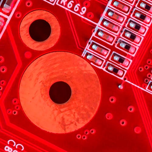
Annular rings of varying sizes on a Class 3 board.
Electrical clearance requirements are largely driven by voltage and the applicable IPC design standard rather than product class alone. However, Class 3 products demand greater manufacturing precision to ensure conductors remain within specified tolerances throughout fabrication.
As PCB feature sizes continue shrinking, even small registration errors can reduce conductor spacing, narrow traces, or shift pads relative to drilled holes. To consistently meet Class 3 acceptance criteria, manufacturers often employ tighter process controls during inner-layer imaging, lamination, optical registration, drilling, and final inspection.
The result is not necessarily smaller minimum trace widths specified by IPC, but greater confidence that the manufactured board matches the designer's intended geometry. For high-density multilayer boards, maintaining registration throughout multiple lamination cycles becomes one of the more demanding aspects of Class 3 fabrication.
Few PCB characteristics create more assembly problems than excessive board warpage. Bow refers to a uniform curvature across the PCB surface, while twist occurs when opposite corners of the board rotate out of the same plane. Excessive bow or twist can interfere with automated assembly, reduce solder joint reliability, and place additional mechanical stress on components after installation.
Because many Class 3 products experience vibration, thermal cycling, or long service lives, IPC limits the amount of allowable board deformation more aggressively than it does for Class 2 products. Maintaining these tighter flatness requirements requires careful control over material selection, copper balance, stackup design, lamination parameters, and cooling rates after pressing.
Engineers often overlook board flatness during layout, yet poor copper distribution or asymmetric stackups can create warpage before fabrication even begins. For Class 3 designs, manufacturability reviews frequently identify these issues early so they can be corrected before production.
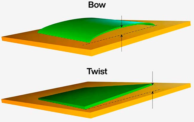
Bow vs. Twist: Bow is a uniform curvature across the PCB surface; twist occurs when opposite corners rotate out of the same plane.
The fiberglass laminate forms the structural foundation of every printed circuit board. Its quality directly influences dimensional stability, dielectric performance, thermal reliability, and resistance to delamination.
While both Class 2 and Class 3 boards may use the same laminate family, Class 3 fabrication places greater emphasis on preserving laminate integrity throughout the manufacturing process. Inspectors evaluate delamination, blistering, resin recession, measling, weave exposure, and internal separation. Many of these conditions may not produce an immediate electrical failure, but they can weaken the board over years of thermal cycling or environmental exposure.
For mission-critical electronics expected to remain in service for decades, preventing these latent defects is just as important as ensuring the board passes electrical testing on the day it ships.
Read more in our PCB Material Reference Guide
Not every PCB failure originates from poor design or defective materials. Microscopic contamination left behind during fabrication can also reduce long-term reliability. Residues from drilling, plating, etching, solder mask processing, or handling may contribute to corrosion, electrochemical migration, dendritic growth, or leakage currents under humid operating conditions.
Class 3 manufacturing places greater emphasis on contamination control, including tighter limits on ionic contamination, residual process chemicals, surface cleanliness, final washing procedures, and handling practices. Although contamination is often invisible to the naked eye, even small amounts of ionic residue can become problematic in harsh environments where moisture and electrical bias combine over extended periods.

Careful handling and contamination control protocols in place for hand soldering
Inspection becomes more rigorous as reliability expectations increase.
Depending on the product, Class 3 fabrication may involve expanded visual inspection, additional microsection analysis to verify plated hole quality, tighter process monitoring, and more comprehensive quality verification throughout manufacturing.

Not necessarily.
Class 3 was developed for products with higher reliability requirements and not for every PCB design.
Commercial electronics, industrial equipment, networking hardware, telecommunications systems, and many medical devices often perform exactly as intended using Class 2 manufacturing standards. Specifying Class 3 for these applications may increase manufacturing complexity without providing meaningful practical benefits.
For aerospace, defense, life-supporting medical equipment, and other mission-critical systems, however, the additional process controls and inspection requirements associated with Class 3 are often fully justified.
The appropriate classification depends on the operating environment, customer requirements, applicable industry standards, and the consequences of product failure.


IPC Class 3 boards are used in mission-critical applications where maximum reliability is required - like military/defense and aerospace
The answer depends on the design. For a simple two-layer PCB with generous spacing and relatively few drilled holes, the cost difference between Class 2 and Class 3 may be modest. For a complex multilayer board with thousands of vias, controlled impedance traces, sequential lamination, or HDI features, the additional process controls required for Class 3 can significantly increase fabrication costs.
In most cases, engineers can expect Class 3 fabrication to cost approximately 20% to 50% more than an equivalent Class 2 board. Highly complex designs may exceed that range depending on material selection, layer count, inspection requirements, and production volume.
The increased cost isn't the result of a single manufacturing step. It reflects dozens of incremental process changes: longer copper plating cycles, additional process monitoring, increased inspection throughout production, higher rejection rates, more stringent workmanship requirements, greater documentation and traceability, and tighter manufacturing tolerances.
Engineers should also consider the indirect costs of specifying Class 3. Fewer fabricators maintain Class 3 certification and process capability, which can reduce supplier options and increase lead times, particularly for complex or quick-turn designs.
The IPC class affects much more than the finished PCB. It influences quoting, design review, manufacturing processes, inspection requirements, documentation, and production planning.
It can also affect the PCB layout itself.
For example, pad sizes and via geometry intended for a Class 2 design may not satisfy Class 3 annular ring requirements. Waiting until fabrication to change the classification can require design revisions that increase project cost and delay production.
Specifying the required IPC class early allows manufacturers to apply the correct fabrication standards from the outset while providing more accurate pricing and lead times.
IPC Class 2 and Class 3 are designed for different reliability requirements, not different levels of manufacturing quality. Class 2 is the right choice for most commercial and industrial electronics, while Class 3 is reserved for applications where long-term reliability and continuous performance are critical.
If you're evaluating which standard is appropriate for your project, the engineering team at San Francisco Circuits can review your design, discuss your application requirements, and recommend the manufacturing approach that delivers the right balance of reliability, performance, and cost.

PCB School
Standards like MIL-PRF-55110, MIL-PRF-50884, and MIL-PRF-31032 exist to enforce reliability, traceability, and performance in environments where failure isn't acceptable.

PCB School
Flying probe testing has been the golden standard of functional testing for low volume, prototype runs since the late 80s and 90s. It effectively flips the approach of the traditional in-circuit (ICT) bed-of-nails fixture test, where a custom-built frame with hundreds of spring-loaded pins contact test points simultaneously.
PCB School
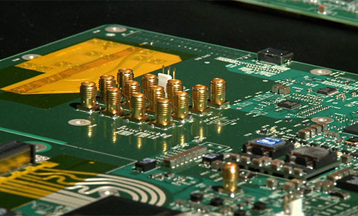
Double-sided Ball Grid Array (BGA) assembly maximizes component density without increasing board size, enabling high-performance designs for applications ranging from smartphones and IoT devices to medical and industrial electronics.
PCB School
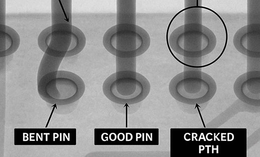
Managing strain during press-fit connector insertion is essential for high-density PCB reliability. Discover best practices and how San Francisco Circuits ensures reliable assembly for HDI, mil-spec, and medical applications.

PCB School
San Francisco Circuits covers the 8 types of PCB vias including blind, buried, microvias, through-hole, stacked, & thermal vias - what they are, how they work, & where they’re used in advanced PCB design.
PCB School
Discover why NIST 800-171 compliance is essential for PCB manufacturers. As a PCB buyer, learn how this cybersecurity framework safeguards your sensitive data & ensure you are engaged with a boardhouse that meets these requirements.