The importance of circuit board stack-ups can often be overlooked. Many times, PCB output files and drawings are riddled with over-constrained dimensions/call-outs, improperly specified parameters, and layer counts/thicknesses based on “best guesses.” We often see PCB stack-ups provided with significant data missing, a situation that leaves critical decisions in the hands of the fabricator and assembler to get it right (although this is more often than not a pretty decent solution).
But no matter the project, big or small, complex or trivial, creating a good stack-up definition can greatly improve long-term reliability and performance, reduce production costs, and allow for a smoother transition to manufacturing.
A PCB stack-up is a high-level outline created before laying out the printed circuit board. It displays the arrangement and details of the layers of the PCB, including the copper and insulating layers.
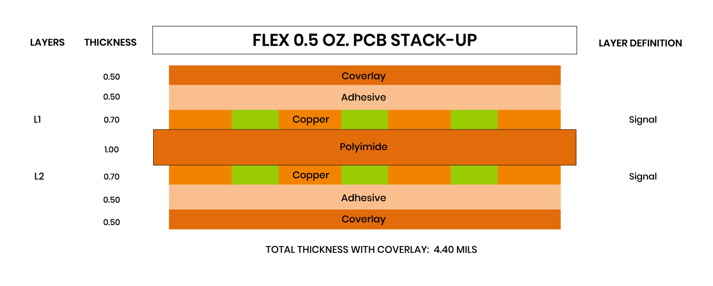
0.5 oz Flex PCB Stack-Up
A PCB stack-up will define copper layer thicknesses & insulating substrate types. PCB layers can contain a range of copper thicknesses, from ½ oz to 2 oz or more. This is pretty understandable since that is how signals and power are managed - the primary purpose of a PCB. But depending on the design requirements, the type of PCB (hybrid, high heat, high speed, etc.) may vary quite a bit and, as a result, the stack-up will look different too.
A very simple single-sided PCB just contains substrate, copper, and soldermask (add a silkscreen for labeling as well). A multi-layer PCB will contain multiple layers of these materials plus prepreg and core. The prepreg is a semi-cured material (such as fiberglass impregnated with resin) that bonds the layers together while the core consists of a fully cured material (like FR4) with the copper laminated to each side.
With multi-layered PCBs, especially high-layer ones with advanced materials and complex requirements, carefully planning and considering the stack-up is absolutely critical.
Use our PCB stackup calculator / design tool to help design and visualize your multilayer PCB stackup from 4 to 14 layers.
Multi-layered boards allow better distribution of energy, cross-interference reduction, while eliminating electromagnetic interference and supporting high-speed signal transfer. These boards also help minimize external noise vulnerability, radiation, and decrease impedance/crosstalk problems.
There are also more exotic PCBs that we specialize in. All of these advanced PCB technologies have special stack-up considerations.
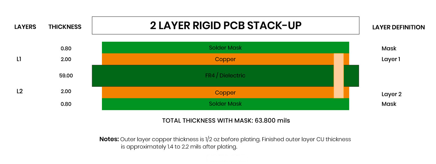
2 Layer Rigid PCB Stack-Up
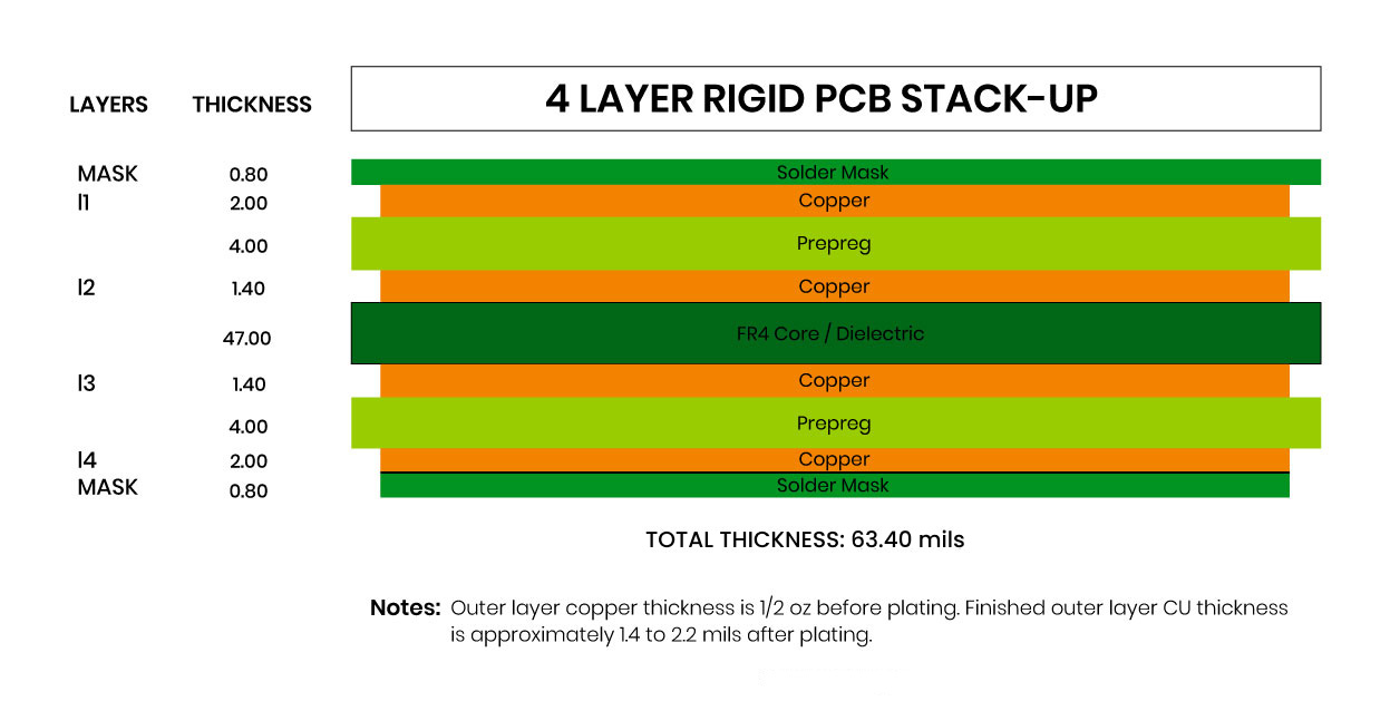
4-Layer PCB Stack-Up
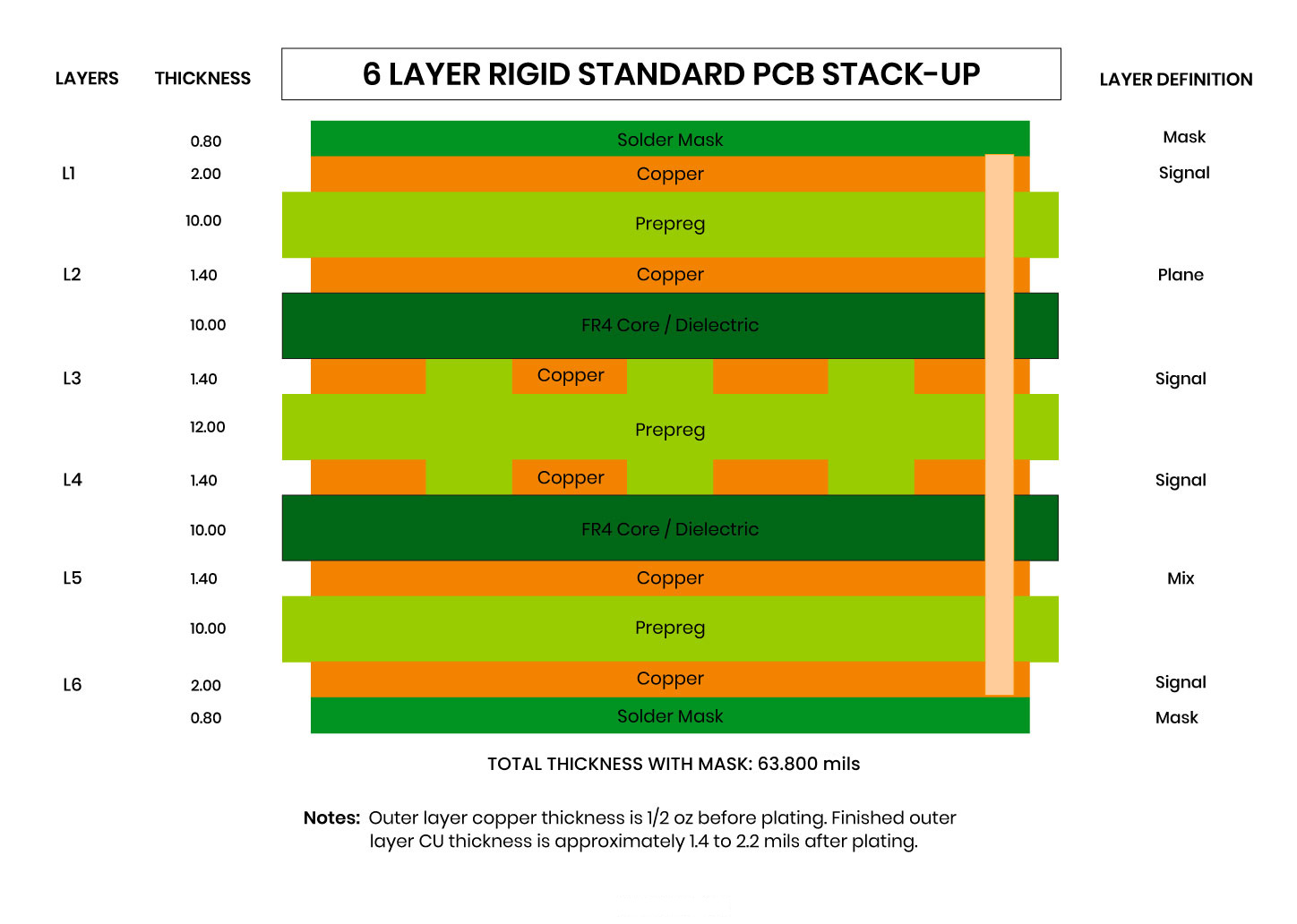
6 Layer Rigid PCB Stack-Up
Metal Core PCBs (MCPCBs) used for high-current LEDs and other high power delivery applications.
The metal core takes up most of the board thickness and provides two purposes. The first is to help take heat away from the junctions of the ICs or components during operation. It also provides a flat, conductive surface on the bottom that can be mounted to external heatsinks.
Read more about metal core PCBs.
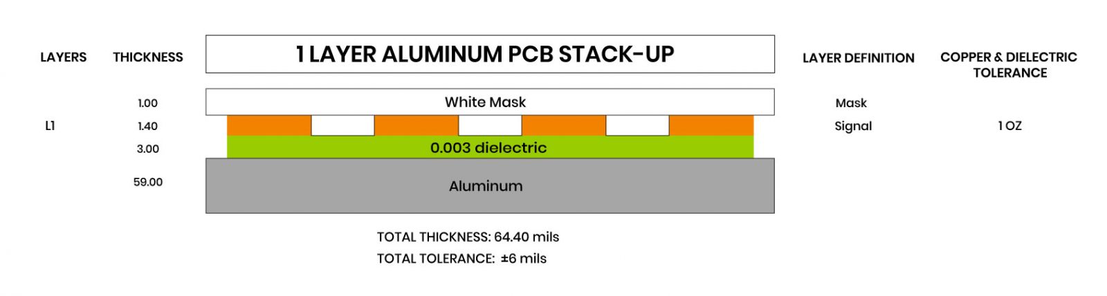
1 Layer Aluminum PCB Stack-Up
High Density Interconnect (HDI) PCBs containing buried, blind, and microvias for ultra compact digital designs. These designs typically contain a high performance processor with very high speed data buses including memory and connections to off-board serial and parallel peripherals like PCI interfacing devices. With very small, non-standard vias, impedance-controlled traces, and high density footprints with tight clearances and soldermask specifications, these boards can contain many layers.
Read more about HDI PCBs.
High Frequency PCBs are for applications that require signal flow rates and frequency ranges up to 100 GHz. These kinds of boards are used primarily for RF-intensive applications and also contain special features like trace antennas and specific tolerances for clearance/spacing and even the amount of solder used on a connector.
Learn more about RF PCBs.
Flex and Rigid-Flex PCBs for small, flexible applications such as wearables and hand-held devices. These kinds of “boards” may just be flex or can be a mix of flex and rigid boards to make up a single circuit board assembly that can bend and move. Flex circuits are made up of a flexible polymer, copper layer (1, 2, or more!) and an overlay, and can utilize planes, traces, and vias just like any other standard PCB.
Read more about Flex PCBs & Rigid Flex PCBs.
0.5 oz Flex PCB Stack-Up
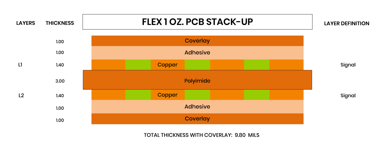
1 oz Flex PCB Stack-Up
Many things will drive the stack-up requirements for a PCB, but the main factors are:
PCB lamination is the stage of PCB fabrication where the inner layers, prepreg, and copper foil are assembled into a multi-layered stack that is laminated together with heat and pressure to complete the multilayer PCB.
There are two ways to laminate a PCB - foil and cap.
Foil construction/lamination is the preferred and the recommended option over cap construction.
In most cases, foil construction is better for layer to layer and drill registration with easier manufacturability with a better yield. The cost is lower since it requires less core laminate material and offers higher yields.
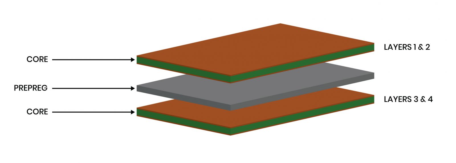
In a foil construction, the prepreg is in between the outer copper layers. For example, on a 4 layer board, it is between layers 1 & 2 at the top as well as in between layers 3 & 4. A continuous sheet of copper foil makes up the outside of the manufacturing panel.
The stack-up below illustrates the foil construction of a 4 layer board, consisting of the following layers from top to bottom:
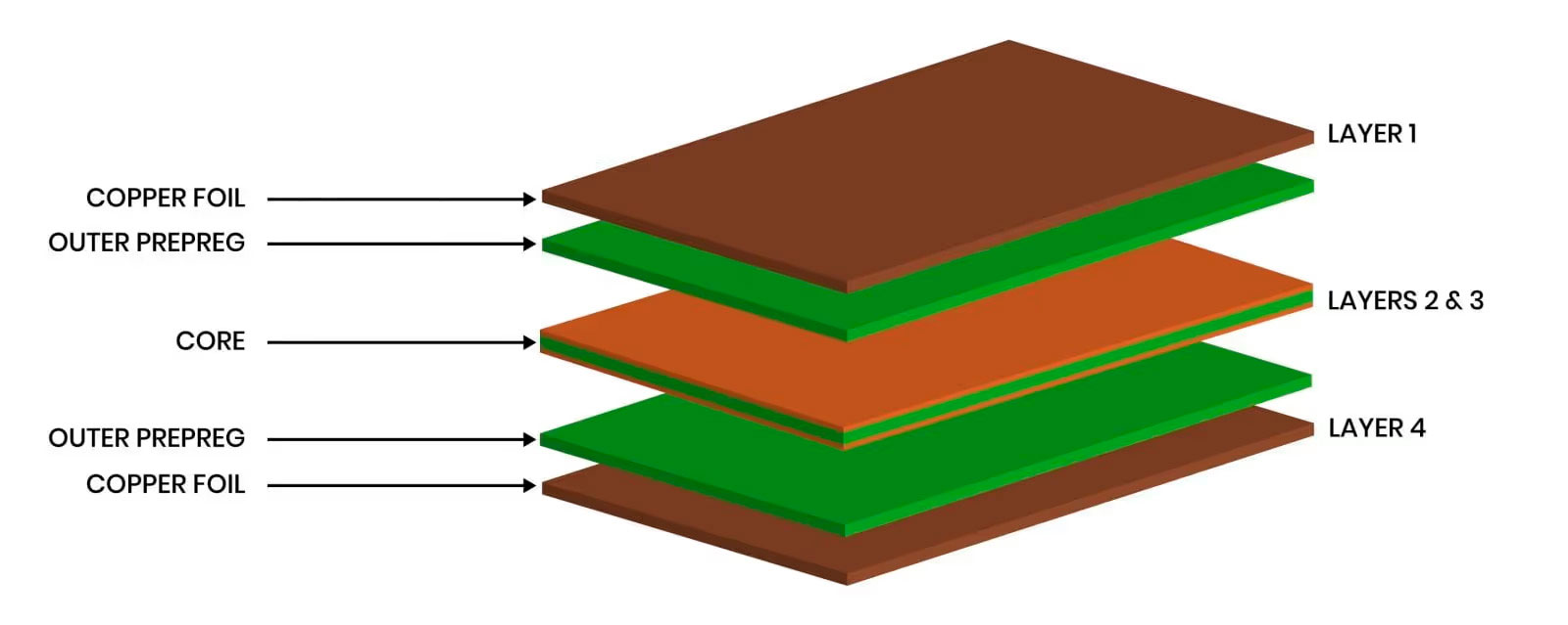
Foil Lamination Stack-Up of a 4 Layer PCB
Note: The prepreg and copper layers are represented as 2 different colors in the stack-up above to visualize how it will be manufactured. In reality, they are the same color as they are usually the same material.
A cap construction has the two outer layers on pieces of pre-copper cladded laminate aka core material to make up the cap layers.
The 4 layer board above would have the outer layers starting with core laminate with a single prepreg layer in between them.
Cap construction is not recommended in modern PCB fabrication. This method is suitable when requirements call for hybrid PCBs with specialty laminates and some blind vias when certain drilling methods are not available, like laser drilling.
The stack-up below illustrates the cap construction of a 4 layer board, consisting of the following layers from top to bottom:
Cap Lamination Stack-Up of a 4 Layer PCB
Overall board density is the most common driver; things like high pin-count processors or memory in Ball Grid Array (BGA) footprints. Depending on the pitch and pinout pattern, it may take several extra layers just to break out the signals from the inner sections of the footprint.
Even though it saves a lot of board real estate, designing with BGA components is sometimes not ideal as it adds more complexity (and cost) during production; in addition to being much harder to rework when needed. The image below shows a 324 pin BGA component that requires several layers for access to each pad.
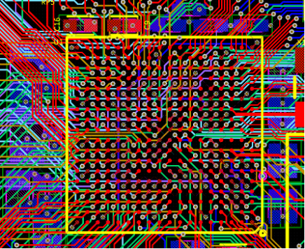
324-pin BGA Component Utilizing 12 Layers
Thermal management is another key driver of stack-up requirements. For PCBs containing many power components or managing high current traces, it may require several layers for power planes/polygons and a lot of copper to help keep resistance down (lower IR drop) or to dissipate power from thermal junctions of components.
Learn more about PCB material selections.
Some RF components (like Modems or RF switches) require several planes to help with power dissipation and improve grounding. Analog intensive boards also may require several ground planes to optimize Signal-to-Noise Ratio (SNR) and reduce Electromagnetic Interference (EMI). And boards with sensitive digital domains like Ethernet, USB, DDR, PCI, etc. may also have dedicated internal layers with extra ground planes.
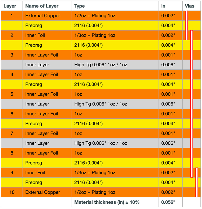
The image below shows a Stack-up editor in Altium Designer consisting of 12 layers and blind/buried vias.
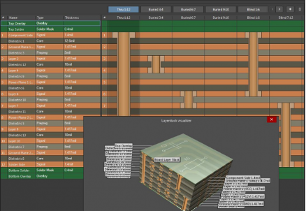
Figure 3. Stack-Up Editor in Altium Designer
There are mechanical reasons for having boards specified at certain thicknesses.
For example, a mechanical engineer might propose 2 layers for a 1 layer board to help provide extra support for thru-hole components. Or perhaps a certain configuration requires a board thickness to be 0.031” (as compared to the standard 0.062”) to help shave off a little bit of height in a stack-up (though be wary of making your boards too thin and keep bow/twist in mind, as it can easily be susceptible to vibration and deflection or warping).
But mechanical requirements aren’t the only things that drive board thickness. Typically, fabricators will have limits on how many layers (depending on their copper pours) they can provide in a given thickness. For PCBs containing 4 layers or less, the standard thickness is 0.062” and it’s typically the lowest cost option. As layer count increases, the minimum thickness will increase as well. For instance, you might be able to have eight 1oz layers on a 0.062” PCB but if the requirements asked for 0.031”, there wouldn’t be enough dielectric material in between layers and the fabricator will reject the design.
Always check with your PCB vendor on capabilities before getting too far in the PCB layout to make sure there aren’t limits in terms of design rules and stack-up. A reputable boardhouse will typically recommend what’s best and present options that balance cost, lead-time/availability, and performance.
Sometimes the designer may specify certain materials but depending on availability and what’s in stock, the PCB provider might suggest a mixture or propose a stack-up that meets a tighter timeline.
Reach out to San Francisco Circuits today to find out how to optimize your stack-up and find that balance between cost, availability/lead-time, and performance.
