The likelihood of a successful assembly run of high-density / fine-pitch circuit boards can be greatly increased through a few simple rules of thumb.
High density or “fine pitch” can be defined as boards with a significantly high amount of components per square inch. That is, the components are extremely close together and the board’s design rules are pushing the limits of PCB fabrication tolerances.
Generally, a high-density application would include very fine-pitch components, which also drives fabrication costs and capabilities. The smaller the component, the smaller its pads (and its actual physical body) which require pick and place machines to be very accurate. When using leadless and grid-array based components, it may require X-ray inspection during the assembly process.
Designing fine pitch circuit boards and applications requires a close relationship between the designer and the board vendor, for a lot of decisions and details depend on the capabilities and equipment offered at the PCB assembly services facility. The PCB supplier should also provide general guidance on risk that can be given by CAM operators and other board house technical representatives.
At San Francisco Circuits, our engineering and support team work with you every step of the way to ensure the most high quality result possible – for both PCB manufacturing and assembly.
High Density PCB Layout Challenges
Laying out a PCB with hundreds of components in a limited amount of space can be a challenging feat that requires a lot of trial and error to avoid issues and pitfalls.
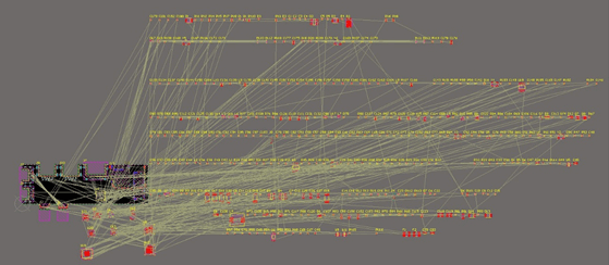
A simple way to illustrate some of the potential pitfalls is with an example. Below is a picture of a circuit board in Altium that contains unplaced components imported from a schematic.
The plan for this board was to populate these components front and back, making it as compact as physically possible, while allowing sufficient room for designing traces and allowing for power planes to carry enough current from one connector to another.
This board also happens to contain USB 3.1 Gen 2 speeds (10Gbps), so there are also considerations for high speed traces and isolation.
This PCB has it all: sensitive high-speed traces, high power path traces (>90W) and a need to be as compact as possible.
To ensure a successful design, each step must be taken one at a time.
The first step, before the PCB layout phase, is to make sure the selected components are small enough to save significant board space during placement. However, this process can end up being a balance between cost savings and board space savings.
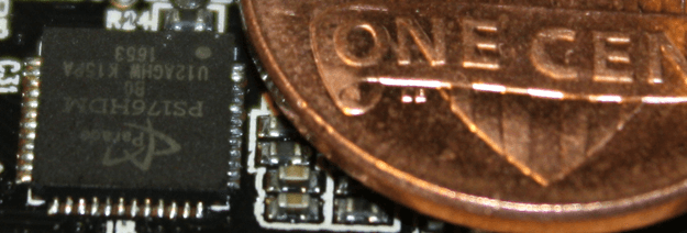
Typically, it costs more during assembly to have finer pitch components populated, especially components requiring specific kinds of inspection, such as grid array based ICs (which require X-Ray inspection). The picture below shows an IC with a pitch of 0.3mm between each pin and compares that to the size of a penny.
As tolerances get tighter, cost goes up, so if the priority is to cut cost, then choosing larger components may end up being the correct approach. Most ICs come in multiple packages and it’s just a matter of looking at the datasheets and considering these things when populating the schematic.
Check out our PCB component overages "cheat sheet" to help you know how many of each component size need to be ordered and at what quantity.
Another aspect to consider for high densities is the rating of each component. A balance is made here as well, weighing the margin desired to build in on things like capacitors to the package size (which is generally driven by power ratings of some sort).
For example, putting a 50V rated capacitor on a 10V rail is not necessary, and you generally want to give a healthy margin of at least 20-30% for capacitor voltage ratings. However, the 10V version of the capacitor, which may be in a much smaller size, would be cutting it too close and leaving no margin. Thus, a 16V rated capacitor may be the best selection, optimizing the size and rating of the capacitor and overall the density of the board itself.
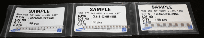
The picture below shows a 1nF capacitor in three different sized packages, each with different voltage ratings:
The same can be said for resistors and power (wattage) ratings. Make sure to size your components appropriately and constantly think of what package you can get away with without introducing risk from underrated components.
The second step to a high-density PCB assembly project, after the schematic and all of its components are specified, is defining a reasonable starting size for the board.
Depending on the mechanical constraints, there may be a physical limit in the X, Y, or Z dimensions due to existing environmental variables that will need to be built in at the start. If the board has a “negotiable” size and the mechanical details are still in development, then then this process is marginally easier.
Typically, the board size will drive the surrounding mechanical hardware (in high-density applications, at least), so the mechanical group will be waiting on some sort of definition and verification that the target board size can even be achieved.
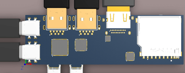
The first step is to check the feasibility of how small the board is likely to be. This is generally done by placing outside connectors, bulky components and large ICs needing some room around them to breakout signals, keeping in mind the need for any sensitive traces and their separation or isolation from the rest of the board. Sometimes cost can be saved when picking preset board sizes/shapes, such as basic square shapes that are fitted to specific dimensions. The following 3D model shows an earlier version of the board pictured previously, and how placing connectors around the edges helps define the size and shape before component placement even begins.
Once the preliminary check out has been completed, ensure the proper design rules are in place, established from the board vendor’s PCB fabrication capabilities.
Considerations include trace width, clearances and via sizes.
There are always trade-offs to consider in terms of cost. There are a few general options that San Francisco Circuits can help you with that balance capabilities with cost. If an end-cost target needs to be met, picking the appropriate design rules at this point is optimal.
At this stage the fine-pitch ICs will have already been determined, which may drive design requirements to some extent. For example, if a BGA component with 0.4mm ball pitch is used, you’ll need to make sure that this spec falls within the capabilities. If high speed ICs that require differential pairs and impedance control are planned on being used, they’ll need to be reviewed with the vendor. If a connector requires various odd-shaped slots, it may fall into a “custom” capability.
Once the design rules are in place and the capabilities are understood, the component placement can begin - fitting components close to each other but with enough room for traces, vias, planes and so on. This becomes mostly trial and error.
Starting with the high-power and high-speed components first is a good idea, along with the connectors and other mechanical components. Once these are placed, it establishes a framework to work from.
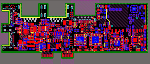
Below is a picture of that same board from above that has been fully populated. Things are extremely tight at this point - so tight that the silkscreen had to be limited to just component outlines and pin orientation, with no reference designators used. This is a common approach that saves board space, as these designators are really only helpful during development or maintenance, and are not necessary during assembly due to pick n place machines and programs that are used. During the placement process, the board grew a little bit in X and Y; it will likely continue to change more from this point as components get routed (could get smaller or bigger).
Additional considerations for board space optimization in fine pitch designs:
Via-in-pads: This is generally recommended against by PCB assembly houses, but can really free up quite a bit of space for traces in between tightly spaced components. The technique primarily consists of building vias on the pads of components (resistors, capacitors, ICs, etc.) to save routing room. However, there is risk that the component will not get an adequate solder connection from the lead to the pad since the via consumes surface area.
Decoupling capacitors: Most of the time, these kinds of components are placed directly above, below or near sensitive pins; and placement is fairly important. However, they can end up consuming a considerable amount of precious board/routing space. In certain cases, some of these capacitors can be left out of the design adding risk for noise on sensitive analog/digital signals (depending on the sensitivity of the IC and how many other capacitors are on the same voltage rail) but the risk may be minimal.
Fiducial marks: Adding these little guide markers for imaging systems allow the pick and place machine to recognize where the PCB is at. They consist of circles (1mm diameter is fairly common) on the top copper layer without solder mask and a circular keepout zone of within 1 diameter’s length away. It’s common to add a couple of these in opposite corners of the PCB. Depending on the placement precision needed for some components, one may even benefit to have them near a very fine pitch IC (such as a processing chip or high pin count FPGA).
These are not required for PCB assembly but greatly help the board assembly vendor with precision placement.
Tooling holes: This is another unnecessary but helpful addition to the PCB for assembly and testing. Tooling holes help with PCB alignment for solder stencils, drilling holes, pick and place machines and test fixtures (when necessary). They can also be used for mounting the board to an enclosure. Board vendors typically have guidelines for these and standard hole sizes that can be used to take advantage of the benefits they might have to offer with tooling/installation.
Special modifications: In order to minimize the volume a bulky or odd-shaped component takes up, it may be worth manually trimming off portions of a component. These portions may include unnecessary metallic shielding, posts that extend beyond the opposite side of the board and other features protruding from a component (usually connectors).
3D parts: Powerful CAD programs can import detailed STEP files of connectors and other mechanical-based components, allowing precision placement and planning. This allows the engineer to minimize clearance between the component pads and the board edge or the clearance between two components.
Test points: The last thing to keep in mind while designing for high-density applications is the ability to test every signal associated with fine-pitch parts. Even with inspection and precision automation, at times even board houses make mistakes and catching them during testing before they leave the facility can save money and time. Providing test points is highly recommended for at-risk signals, and can reveal shorts, opens, components installed backwards or other anomalies.
There is almost always a balance between cost and complexity when it comes to PCB fabrication and assembly, and knowing the trade-offs could save you considerable money and time during the development and production of a product.
