In today’s applications where designs are commonly becoming faster and faster, controlling layout parameters is more critical than ever.
There are several ways to approach impedance control during PCB design and production. The most common way is to annotate the information inside the schematic with symbols and special notes, incorporate these notes and design rules when laying out the PCB, and describe it via a PCB fabrication drawing so that your PCB vendor knows about it and can fabricate it appropriately.
Why is it necessary? Simply put, a signal with a given amount of energy and speed will leave a component’s output pin, travel through a PCB trace and end at another component’s input pin.
If the signal’s energy is not fully absorbed by the receiving end, some of the left-over energy can be reflected back onto the trace and travel back to the output pin. These reflections may cause interference with the real signal and lessen the overall signal integrity.
For very short traces, you may not need to worry about controlling impedance but, as a general rule of thumb, any traces longer than 1/10th the wavelength of the signal should incorporate some sort of controlled impedance.
Another general rule of thumb is to incorporate controlled impedance on a trace whose length is longer than 1/3 the rise time of the signal. High Speed USB, Ethernet, DDR Memory, and other low-voltage, differential communication systems are examples of data rates at which require impedance control.
A trace has several characteristics to consider: height, width, length, distance between itself and other copper features (including copper layers beneath or on top of the signal layer containing controlled impedance), the dielectric constant, PCB fabrication tolerances/limits, etc. All of these are considered when calculating and designing for controlled impedance. Most industry-standard CAD software has impedance control and differential pair feature sets that calculate these things for you (and even simulations that can show you expected signal integrity and any potential issues), but knowing how they all play together can help better understand when it is necessary or not.
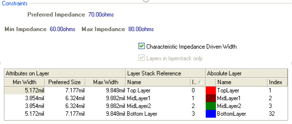
Here is a screenshot from Altium Designer (taken from Altium TechDocs) on a 4-layer board containing some simple 70-ohm impedance-driven trace widths:
These days, controlling impedance is typically done at the board house with modelling software and testing impedance on bare boards upon production, but knowing how to call these specifications out in a drawing is important for the PCB designer as well.
This can usually be accomplished by annotating the PCB drawing with a note and arrow pointing to the trace (or group of traces) on the board, stating that “7mil width and 8mil space layers 1 and 8 require differential impedance of 90 Ohms”, along with the layer stack-up legend and its requirements regarding copper thickness and dielectrics.

PCB School
Standards like MIL-PRF-55110, MIL-PRF-50884, and MIL-PRF-31032 exist to enforce reliability, traceability, and performance in environments where failure isn't acceptable.
PCB School
Flying probe testing has been the golden standard of functional testing for low volume, prototype runs since the late 80s and 90s. It effectively flips the approach of the traditional in-circuit (ICT) bed-of-nails fixture test, where a custom-built frame with hundreds of spring-loaded pins contact test points simultaneously.
PCB School
Double-sided Ball Grid Array (BGA) assembly maximizes component density without increasing board size, enabling high-performance designs for applications ranging from smartphones and IoT devices to medical and industrial electronics.
PCB School
Managing strain during press-fit connector insertion is essential for high-density PCB reliability. Discover best practices and how San Francisco Circuits ensures reliable assembly for HDI, mil-spec, and medical applications.

PCB School
San Francisco Circuits covers the 8 types of PCB vias including blind, buried, microvias, through-hole, stacked, & thermal vias - what they are, how they work, & where they’re used in advanced PCB design.

PCB School
Discover why NIST 800-171 compliance is essential for PCB manufacturers. As a PCB buyer, learn how this cybersecurity framework safeguards your sensitive data & ensure you are engaged with a boardhouse that meets these requirements.
