Via tenting is the application of soldermask to encase or seal the via’s opening. A via is essentially a hole drilled into the PCB that facilitates connections between multiple PCB layers. An untented via, on the other hand, remains uncovered by a soldermask layer. The decision to expose or cover these vias carries both advantages and disadvantages contingent upon your specific design and manufacturing requirements.


Tented via (left) and untented via (right) of a board showing the differences in soldermask covering the vias.
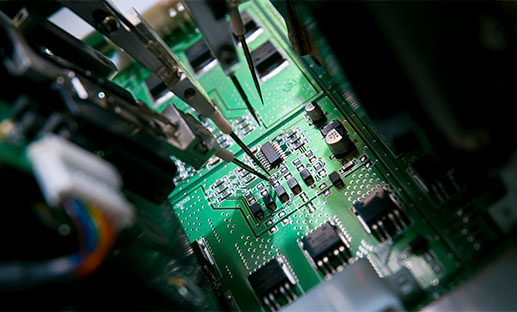
Soldermask typically takes the specific form of Liquid Photo Imageable (LPI). LPI soldermask is a curable two-part compound applied through a screen printing process onto the PCB through UV, oven, or heat.
It is then subjected to UV curing to achieve a durable finish. This soldermask serves as a crucial physical barrier, safeguarding the PCB's copper layers. It boasts a high electrical isolation rating, typically around 2.5 × 10¹² Ω.
The primary role of a PCB's soldermask is to shield the copper traces from potential damage, oxidation, and solder bridging. This safeguarding extends to the vias as well. Tenting vias enhances their resistance to physical damage and electrical shorts.
For PCB designs incorporating through-hole components to be wave soldered, tented vias prevent solder from flowing into the via and causing short circuits on the opposite side of the PCB. Vias situated near SMT (Surface Mount Technology) pads should also be tented to prevent solder paste from wicking into the via, leading to suboptimal solder joints. This is especially crucial for BGA (Ball Grid Array) designs employing "dogbone" escape routing.
Tented vias also prevent entire pads from being exposed under BGA, which creates a higher risk for a short because excess solder can flow from the pad to the via. These risks are even greater in double-sided BGA assembly, where BGAs are populated on both sides of the PCB and reflow sequencing, inspection access, and solder containment become significantly more challenging.
Read more about reflow soldering here.
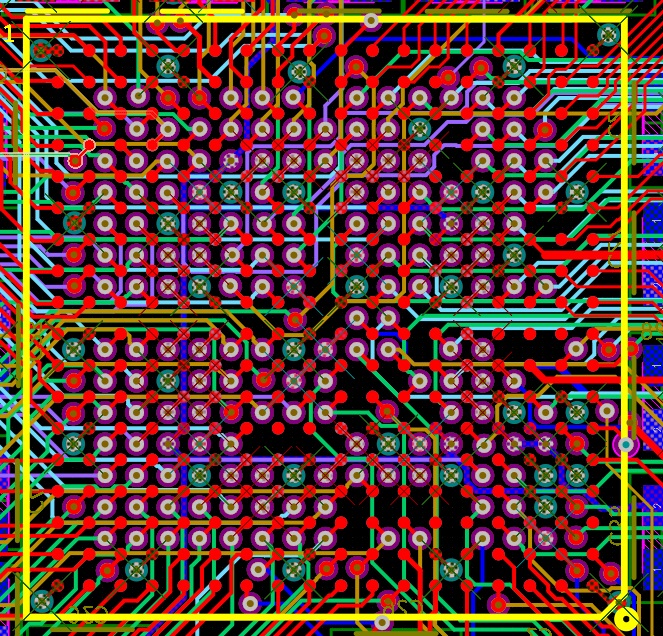
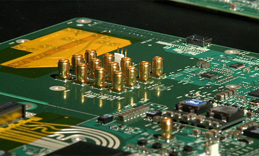
A BGA component on a 12-layer board requiring vias for nearly every single pin.
These vias must be tented given the close proximity to pads and risk for solder bridges.
Nonetheless, tenting vias does present certain downsides. Because the LPI soldermask is a liquid, it needs to bridge the gap over the via hole, potentially leaving a small opening. This opening could permit corrosive flux, moisture, or other chemicals to infiltrate the via, posing a risk of copper corrosion. This concern is lessened, but not eliminated, by the prevalence of "no clean" flux in SMT assembly compared to corrosive "water clean" flux.
Leaving vias exposed without soldermask does not imply that the copper is exposed to the environment. The exposed vias are plated with the PCB's surface finish.
ENIG and ENEPIG finishes will coat the interiors of exposed vias with gold, guarding against corrosion and damage. During the prototyping phase, exposed vias can be extremely beneficial for troubleshooting, trace adjustments, and ad-hoc test points.
Read more about PCB surface finishes here.
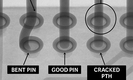
Vias, when left untented, may have a risk for bridging solder next to pads
Shown above: one pad is a test point that is to be hand-soldered, another pad is from a resistor)
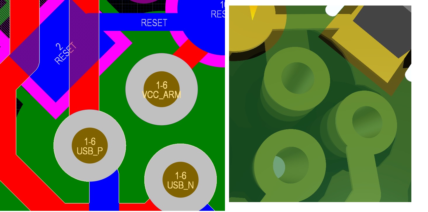
When soldermask is applied to holes, it can trap and leave chemicals in the hole. Tented vias can also have tent breaks, leading trapped chemicals to seep in and also get trapped. This is why manufacturers employ a technique called “barrel relief”, where the majority of the pad is tented but the two barrel holes are left exposed on both sides of the PCB. Both the ENIG and ENEPIG surface finishes will plate inside of the holes and prevent additional chemicals from getting trapped inside.
If barrel relief is only applied to one opening of the PCB, instead of both, chemicals can still get trapped in the hole similar to the way a cup holds water. Trapped, corrosive chemicals may eat away at the hole wall and create an open circuit. To prevent long-term reliability issues, manufacturers apply the barrel relief to avoid exposing the entire pad.
Barrel relief prevents the solder from wicking onto the holes when the vias are close to an SMT pad. The soldermask clearance for the via and SMT pad overlap, but the exposed copper area is protected due to the barrel relief.
If tented from both sides, there's still technically some air trapped between the two tents. This air can sometimes expand at assembly potentially leading to the broken tent issue and the trapping of flux. Also, this air in space applications can expand, which is considered outgassing. Any type of contaminants that were in there, can cause critical issues when settling on adjacent image sensors or other sensors in space.
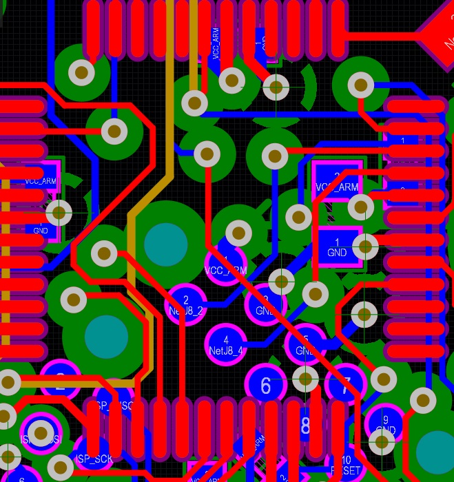
A large component that contains many vias underneath. Although the component doesn't have any kind of thermal pin/pad underneath, there is still risk that some solder can wick to an untented via underneath a component and get missed during the visual inspection of a part.
So, the pivotal question remains: should you tent your vias or leave them exposed?
For long-term PCB reliability and enhanced manufacturability, it is generally advisable to fully encase the vias, preventing moisture and fluids from entering. Corrosive and trapped liquids cause copper corrosion while tent breaks can also lead to trapped, harmful chemicals. Tented vias, and those created with barrel relief, can help prevent these prevalent issues.
However, the cost-effectiveness of this approach can be a concern when simpler solutions are readily available. Smaller vias are more amenable to effective tenting, with a threshold typically around 15-mil diameter.
Vias larger than 15 mils should be left exposed, relying on the surface finish for sealing. Ensure that vias under BGA components or those adjacent to SMD pads are tented, while those further away can often remain exposed in your PCB design.
PCB School
Standards like MIL-PRF-55110, MIL-PRF-50884, and MIL-PRF-31032 exist to enforce reliability, traceability, and performance in environments where failure isn't acceptable.
PCB School
Flying probe testing has been the golden standard of functional testing for low volume, prototype runs since the late 80s and 90s. It effectively flips the approach of the traditional in-circuit (ICT) bed-of-nails fixture test, where a custom-built frame with hundreds of spring-loaded pins contact test points simultaneously.
PCB School
Double-sided Ball Grid Array (BGA) assembly maximizes component density without increasing board size, enabling high-performance designs for applications ranging from smartphones and IoT devices to medical and industrial electronics.
PCB School
Managing strain during press-fit connector insertion is essential for high-density PCB reliability. Discover best practices and how San Francisco Circuits ensures reliable assembly for HDI, mil-spec, and medical applications.
PCB School
San Francisco Circuits covers the 8 types of PCB vias including blind, buried, microvias, through-hole, stacked, & thermal vias - what they are, how they work, & where they’re used in advanced PCB design.

PCB School
Discover why NIST 800-171 compliance is essential for PCB manufacturers. As a PCB buyer, learn how this cybersecurity framework safeguards your sensitive data & ensure you are engaged with a boardhouse that meets these requirements.
