PCB line spacing is relevant to both safety and function when it comes to traces. Comprised of copper, fuses, and insulation, a trace is a conductive connection between different components on a PCB. Numerous factors determine the effectiveness of tracing, including PCB trace widths.
By connecting various signals, the trace serves as an important connection with its own sets of benefits and avoidable drawbacks.
Line tracing allows the signals to travel between different components. They’re beneficial but also prone to issues, as they’re susceptible to potential errors that could lead to a malfunction. But for products or circuit boards using high voltages, safety standards are extremely relevant. As line spacing between different conductive components increases, so do spacing standards. If the breakdown voltage is exceeded when safety standards aren’t adhered to, arcing could occur along the board, presenting issues between the traces.
As technology continues to evolve, so do the standards by which it’s created. Designers have more capability and tools than ever, but high-voltage circuitry poses a number of challenges. When mixing any technologies, or creating important PCBs used for medical equipment or similar devices, accurate line spacing is a necessity. Over time, these practices have also been used to reduce product sizes and ultimately create more precise circuitry.
|
Voltage Between Conductors (DC or AC Peaks) |
Minimum Spacing | ||||||
| Bare Board | Assembly | ||||||
| B1 | B2 | B3 | B4 | A5 | A6 | A7 | |
|
0-15 |
0.05 mm |
0.1 mm |
0.1 mm |
0.05 mm |
0.13 mm |
0.13 mm |
0.13 mm |
|
16-30 |
0.05 mm |
0.1 mm |
0.1 mm |
0.05 mm |
0.13 mm |
0.25 mm |
0.13 mm |
|
31-50 |
0.1 mm |
0.6 mm |
0.6 mm |
0.13 mm |
0.13 mm |
0.4 mm |
0.13 mm |
|
51-100 |
0.1 mm |
0.6 mm |
1.5 mm |
0.13 mm |
0.13 mm |
0.5 mm |
0.13 mm |
|
101-150 |
0.2 mm |
0.6 mm |
3.2 mm |
0.4 mm |
0.4 mm |
0.8 mm |
0.4 mm |
|
151-170 |
0.2 mm |
1.25 mm |
3.2 mm |
0.4 mm |
0.4 mm |
0.8 mm |
0.4 mm |
|
171-250 |
0.2 mm |
1.25 mm |
6.4 mm |
0.4 mm |
0.4 mm |
0.8 mm |
0.4 mm |
|
251-300 |
0.2 mm |
1.25 mm |
12.5 mm |
0.4 mm |
0.4 mm |
0.8 mm |
0.8 mm |
|
301-500 |
0.25 mm |
2.5 mm |
12.5 mm |
0.8 mm |
0.8 mm |
1.5 mm |
0.8 mm |
|
> 500 |
0.0025 mm |
0.005 mm |
0.025 mm |
0.00305 mm |
0.00305 mm |
0.00305 mm |
0.00305 mm |
B1 - Internal Conductors
B2 - External Conductors, uncoated, sea level to 3050 m [10,007 feet]
B3 - External Conductors, uncoated, over 3050 m [10,007 feet]
B4 - External Conductors, with permanent polymer coating (any elevation)
A5 - External Conductors, with conformal coating over assembly (any elevation)
A6 - External Component lead/termination, uncoated, sea level to 3050 m [10,007 feet]
A7 - External Component lead termination, with conformal coating (any elevation
Source: IPC-2221B conductor spacing requirements
As PCBs have become even more complex and precisely designed, the minimum trace spacing becomes even more relevant. That is the minimum distance needed for a trace or other components to withstand a specific voltage.
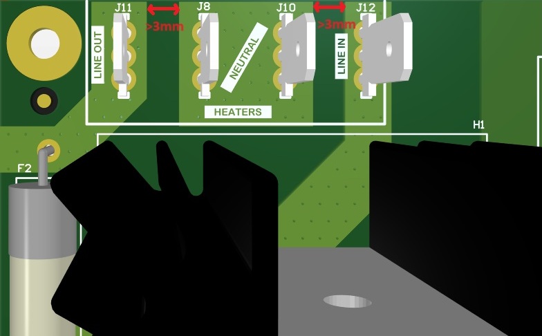
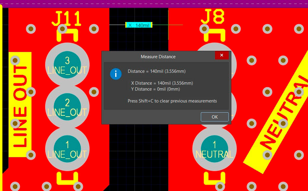
Design with 240VAC input power and >3mm creepage spacing
Clearance and creepage are now more than important safety practices, they’re internationally-required safety standards. Ultimately, both creepage and clearance are used to prevent arcing. Those standards need to be followed regarding high-voltage circuitry, for both safety and functionality, or the PCB and the product it’s in will experience issues.
Creepage considerations are important in all applications and voltages. PCB designers can often overlook the need for creepage at lower, DC-based voltages, which can sometimes get them in trouble. It's especially important around connectors and exposed pads that are placed too close together.
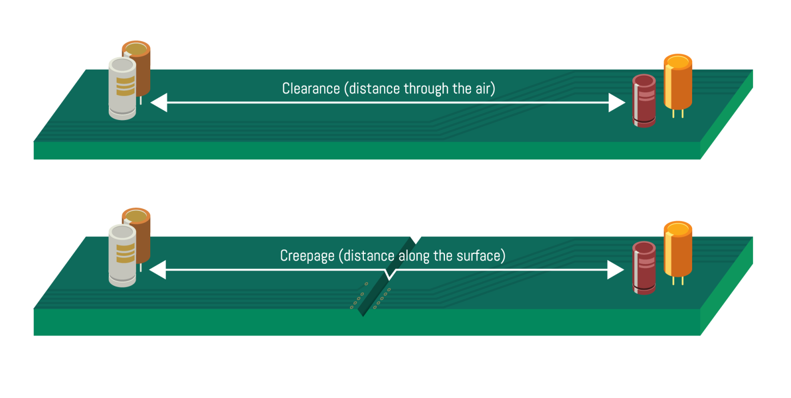
The shortest distance in the air between conductive parts is otherwise known as clearance. By measuring the shortest path that doesn’t pass through insulation, parts, or sleeving clearance can then be evaluated. Environmental effects are extremely relevant to clearance, especially when humidity can increase the chance of arcing, as both moisture and humidity could lead to arc flashes. Dust or other small particles can also cause issues between the conductive components.
Similar to clearance, creepage is the same measurement between conductive parts except they must be along the surface of some kind of insulation. They also have similar requirements and concerns with the only difference being the insulation of the creepage instead of the air that clearance passes through
The only difference in these is regarding the surface along which the current travels, with creepage going through an insulated surface while clearance passes through air. When factoring in the individual specifications clearance and creepage distance are typically very similar. The only instance where there would be a difference is concerning high-voltage circuits that may require different clearances and components.
There are several safety regulations that pertain to creepage and clearance. They provide clear direction on how to operate equipment under ideal conditions and temperatures, and detail how to manufacture high-quality equipment and parts in a safe environment.
The standards laid out in IPC-2221 detail numerous requirements designed to prevent issues related to overheating and thermal management. They ensure that a proper trace width is calculated to keep the relevant temperature below their thresholds. This is a widely accepted standard that not only lays out best practices but also the ideal materials.
Relevant to power conversion, this dictates the safety standards specifically for PCDs. By creating a standard power for computers and other communication devices this creates a safety net by which PCB creators can analyze their spacing requirements based on voltage and whether it’s an external or internal layer.
This safety standard regards the appropriate distances for clearance and creepage for laboratory and industrial equipment. For equipment used for measuring, and controlling processes like pH controllers or temperature, poorly measured distances pose a massive risk. Suggested measurements are laid out in BS EN 61010-1:2010 standards (Safety requirements for electrical equipment for measurement, control, and laboratory use - General requirements), including those found in the table that follows.
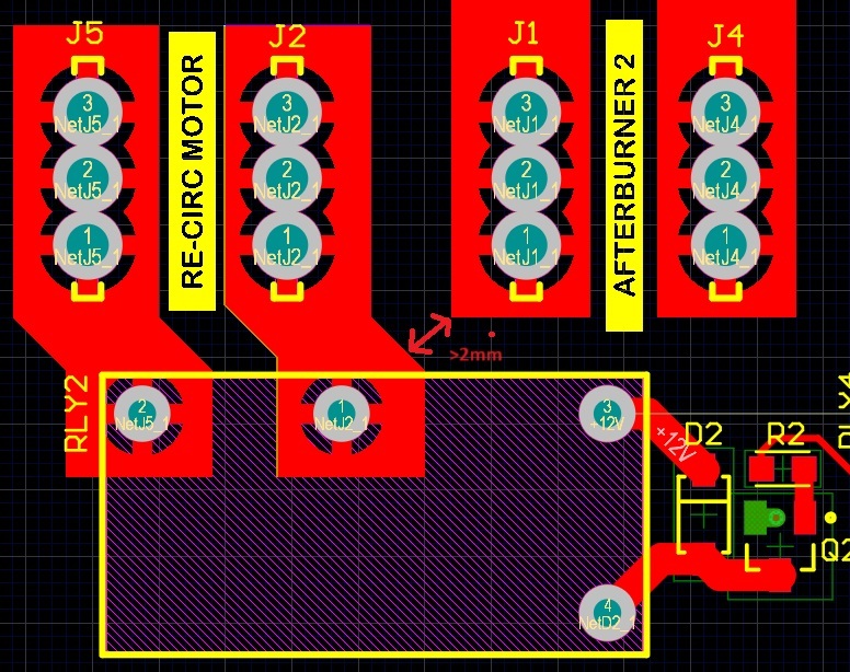
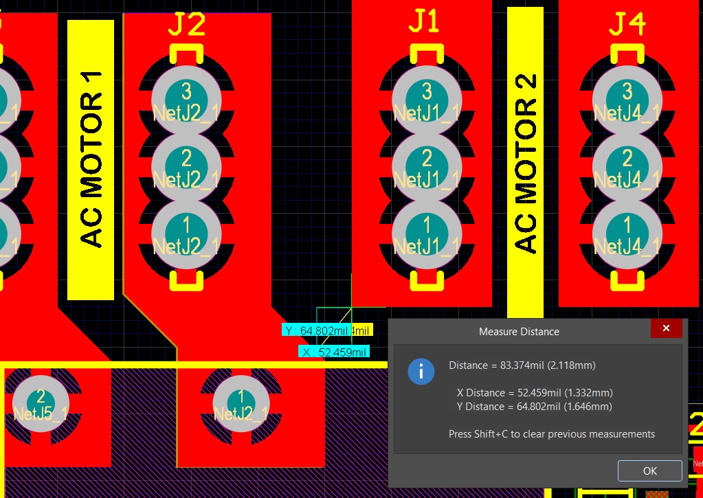
Design with multiple 120VAC motors which are separated by >2mm creepage spacing
|
Voltage line-to- neutral a.c. r.m.s. or d.c. |
Values for CLEAR- ANCE |
|||||||||
| Values for CREEPAGE DISTANCE | ||||||||||
|
Printed wiring board material |
Other insulating material | |||||||||
|
Pollution DEGREE 1 |
Pollution DEGREE 2 |
Pollution DEGREE 1 |
Pollution DEGREE 2 |
Pollution DEGREE 3 |
||||||
|
All material groups |
Material group I, II, IIIa |
All material groups |
Material group I |
Material group II |
Material group III |
Material group I |
Material group II |
Material group III |
||
|
V |
mm |
mm |
mm |
mm |
mm |
mm |
mm |
mm |
mm |
mm |
|
≤150 |
0.5 |
0.5 |
0.5 |
0.5 |
0.8 |
1.1 |
1.6 |
2.0 |
2.2 |
2.5 |
|
>150≤300 |
1.5 |
1.5 |
1.5 |
1.5 |
1.5 |
2.1 |
3.0 |
3.8 |
4.1 |
4.7 |
EN 61010 safety standard: clearances and creepage distances for mains circuits of overvoltage category II up to 300v
Note:
a) The values in Table 4 are for BASIC INSULATION and SUPPLEMENTARY INSULATION. Values for REINFORCED INSULATION shall be twice the values for BASIC INSULATION.
b) Minimum CLEARANCE for BASIC INSULATION, SUPPLEMENTARY INSULATION and REINFORCED INSULATION for POLLUTION DEGREE 3 is 0.8 mm.
c) If the equipment is RATED to operate at an altitude greater than 2,000 m, the CLEARANCES need to be multiplied by the factors found in Table 3 of the standards document.
Maintaining these standards isn’t just important, it leads to increased functionality and longer use for the components and the PCB itself. However, this doesn’t address or solve every potential issue with creepage or clearance.
Calculating the necessary clearance and creepage is just the first step in a complicated process. Temperature, air pollution, moisture, humidity, and voltage are all different variables that will affect the PCB. These are a short set of guidelines to help avoid concerns and issues when determining creepage and clearance specifics.
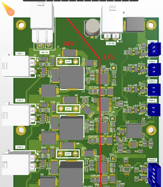
Top-down view of a design containing 48VDC. Creepage should apply to every design, even lower voltages such as 48VDC.
For high-voltage PCBs and connections, more demands will be required of the PCB materials and components. They’ll be more susceptible to voltage fluctuations, exposure to different environments and humidities, and potential overvoltage as the product degrades over time. That’s why it’s incredibly important to use circuits that are specifically recommended and designed for clearance and creepage.
High-voltage circuits that operate at a minimum of 50V will need longer distances for both clearance and creepage to prevent electrical issues and breakdowns. Read more about RF PCBs here.
Medical devices often have more failsafes than other industrial equipment. Both kinds of distances need to be strictly adhered to and specified because of the importance and significance of the devices. Components, use, and interaction with patients are all factors for clearance and creepage in medical equipment.
OSHA and other governing bodies have put strict specifications on industrial equipment and devices that need to be adhered to, especially those that account for particulates like dust, heat, and vibration/movement.
The higher the voltage and power of a device the higher the risk is of problems. When dealing with high currents and voltage, longer clearance and creepage distances are typically required to avoid issues with arcing, insulation, and voltage faults.
For materials, every component needs to be carefully selected. High operating voltages will be a factor, so not only does there need to be accurate spacing, but 2oz minimum traces or vias of copper and resin and glass levels are known to provide the durability and reliability required for those high-voltage projects and products.
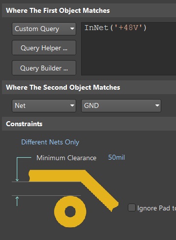
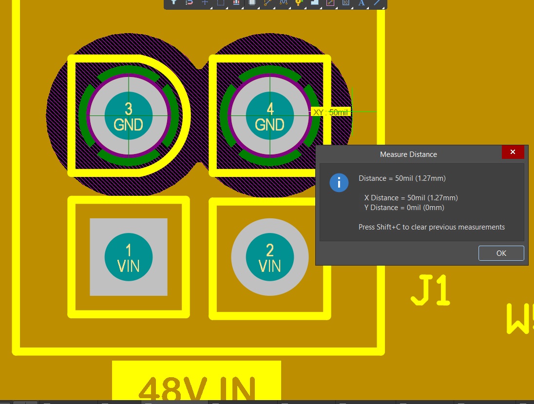
How to set design rules in Altium with result (right) shown on traces, planes, and polygon pours; found on same 48V input power connector (50mils or >1mm between 48V and ground)
Standards and practices are becoming more unique and more specific to the job or project they’re used for, and that’s only going to continue as technology continues to evolve. While hobby PCB creation is fun and fulfilling, many professional PCBs are used from modern industrial tools to life-saving devices. That’s why precise line spacing is such an important and meticulous detail.
Maintain these practices and utilize these materials and you’re one step closer to stable, high-voltage PCBs.
PCB School
Standards like MIL-PRF-55110, MIL-PRF-50884, and MIL-PRF-31032 exist to enforce reliability, traceability, and performance in environments where failure isn't acceptable.
PCB School
Flying probe testing has been the golden standard of functional testing for low volume, prototype runs since the late 80s and 90s. It effectively flips the approach of the traditional in-circuit (ICT) bed-of-nails fixture test, where a custom-built frame with hundreds of spring-loaded pins contact test points simultaneously.
PCB School
Double-sided Ball Grid Array (BGA) assembly maximizes component density without increasing board size, enabling high-performance designs for applications ranging from smartphones and IoT devices to medical and industrial electronics.
PCB School
Managing strain during press-fit connector insertion is essential for high-density PCB reliability. Discover best practices and how San Francisco Circuits ensures reliable assembly for HDI, mil-spec, and medical applications.

PCB School
San Francisco Circuits covers the 8 types of PCB vias including blind, buried, microvias, through-hole, stacked, & thermal vias - what they are, how they work, & where they’re used in advanced PCB design.

PCB School
Discover why NIST 800-171 compliance is essential for PCB manufacturers. As a PCB buyer, learn how this cybersecurity framework safeguards your sensitive data & ensure you are engaged with a boardhouse that meets these requirements.
