Today's world is filled with embedded applications and densely populated circuitry. Just about every widget these days has some sort of electronics, likely running on embedded code (firmware). In order to get that firmware loaded to the circuit board, a programming port is generally used (at least initially during production) and those ports can be very bulky (and costly) relative to most other components on the board, and sometimes even drive the size of a board or enclosure.
What if you didn't need that programming connector in your designs? How much smaller could the device be? Smartphones are the epitome of what would be considered a design where not one square micron of space is wasted. Why not your design? And how else can you reduce unnecessary space and cost in a product by replacing connectors with an alternative connection?
Processors, BLE modules, WiFi chips, anything that is programmable requires some step of physically loading code, even if running on bootloaders and allowing for remote or over-the-air firmware updates. And generally, a designer or developer will want a connection in place to not only load code but also allow for system debugging using powerful hardware and software tools associated with the processor. These connections often need to mate with debugger cables that have bulky plugs, and sometimes costly mating connectors.
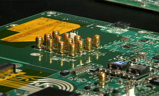
In a design where every bit of space and cost counts, replacing this programming connection with a group of exposed copper pads could make a significant difference. Tag-Connect has done an excellent job of developing a product that does just that: by replacing JTAG and other common programming connections with a small pattern of exposed, circular copper pads that interface with pogo pins (spring-loaded contacts that you can hold in place manually, or clip on if the connection supports it). There are other brands of cables that have built-in pogo pins but the general concept here is to convert bulky header-based connections to smaller, zero-profile connections that free up board space and cost.
2D footprint in Altium Showing the Tag-Connect TC2050 Connection
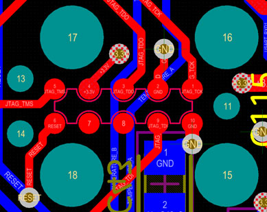
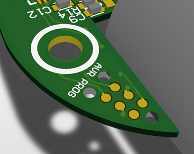
Below is an example of a pogo-pin footprint for programming a processor: the Tag-Connect 10-pin legged TC2050. This one has other thru-holes (the bigger teal circles) associated with it that allow clips to secure the pogo pins in place so that the user can operate hands-free. The smaller circles (11, 13, and 14) are there to assist in aligning the pogo pins.
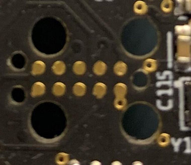
Actual footprint of TC2050 on a Printed Circuit Board
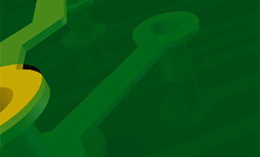
There may be instances where you don’t have the luxury of having alignment or clip holes if there are components or mechanical interferences on the other side of the board, or if things are too compact. In that case you can operate without the clips, or just have trimmed alignment posts that only extend through the alignment holes. Here’s an example of a 6-pin Tag-Connect footprint with just the alignment holes in a relatively tight space.
6-pin legless Tag-Connect footprint in Altium 3D
And the picture below shows an instance where this same footprint is used on a board that has a mechanical component on the opposite side, block 2 of the 3 alignment holes. And the picture below shows an instance where this same footprint is used on a board that has a mechanical component on the opposite side, block 2 of the 3 alignment holes.
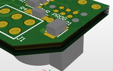
6-pin legless Tag-Connect footprint in Altium 3D with component on opposite side
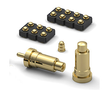
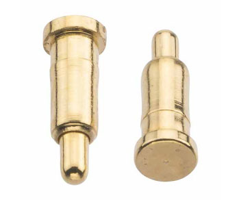
But why limit this to just programming ports? What about spare connections? Debug connections? Test points (that were previously connector-based)? Anything that doesn’t have a normal connection during operation or general use, that might only require a temporary connection at some point. Flying probe test fixtures and “bed-of-nail fixtures” have been around for decades and the main method of probing involves pogo pins touching down on test pads, exposed vias, or even component pins and it’s just another very easy, low-cost and low-profile way to access board connections without the use of headers. Spare or test connections utilizing pads for pogo-pin interfacing can be a very low-profile way of bringing up a design, or testing it in a production environment. There’s really no limit to what a pogo-pin interface can look like. A variety of individual pogo pins exist today as an off-the-shelf solution for both cable or Printed Circuit Board (PCB) integration, such as those from Mill-Max or Harwin:
It’s common to incorporate these on a test or debug PCB that might be utilized during a design or production process, typically if you want to run a functional test or probe a group of signals accessed by small exposed copper pads. These pads can be very close together and occupy minimum board space, a great way to save real estate in a space-conscious design. In order to better manage temporary, external connections by saving cost and board space, and creating a quicker, more reliable means to test or debug a PCB, consider adding pogo-pin-based connections to your design today.
At San Francisco Circuits, we would like to connect with you to learn more about your specific needs and also bring your PCB product into reality. We look forward to connecting with you soon!
PCB School
Standards like MIL-PRF-55110, MIL-PRF-50884, and MIL-PRF-31032 exist to enforce reliability, traceability, and performance in environments where failure isn't acceptable.
PCB School
Flying probe testing has been the golden standard of functional testing for low volume, prototype runs since the late 80s and 90s. It effectively flips the approach of the traditional in-circuit (ICT) bed-of-nails fixture test, where a custom-built frame with hundreds of spring-loaded pins contact test points simultaneously.
PCB School
Double-sided Ball Grid Array (BGA) assembly maximizes component density without increasing board size, enabling high-performance designs for applications ranging from smartphones and IoT devices to medical and industrial electronics.
PCB School
Managing strain during press-fit connector insertion is essential for high-density PCB reliability. Discover best practices and how San Francisco Circuits ensures reliable assembly for HDI, mil-spec, and medical applications.
PCB School
San Francisco Circuits covers the 8 types of PCB vias including blind, buried, microvias, through-hole, stacked, & thermal vias - what they are, how they work, & where they’re used in advanced PCB design.

PCB School
Discover why NIST 800-171 compliance is essential for PCB manufacturers. As a PCB buyer, learn how this cybersecurity framework safeguards your sensitive data & ensure you are engaged with a boardhouse that meets these requirements.