There are several factors that drive trace width, length, and style during the PCB design process of your next PCB prototype. This article will dive into a variety of applications that demand specific trace layout characteristics and how or when to incorporate them into your PCB design.
Let’s start with the basics. What exactly is trace width and why is specifying a particular trace width so important? The point of a PCB trace is to connect any kind of electrical signal, whether it be analog, digital, or power, from one junction to another.
The junction can be the pin of a component, a branch off of a larger trace or plane, or an empty pad or test-point intended for probing. Trace widths are often measured in mils, or thousands of an inch. A standard trace width for an ordinary signal (no special requirements) may be in the 7-12 mil range and be as long as a few inches, but there are many things that should be considered when defining the width and length of a trace.
The application will often drive the trace widths and types in a PCB design and at a certain point, there is usually a balance with regards to PCB fabrication cost, board density/size, and performance. If a board has specific design requirements such as speed optimization, noise or coupling mitigation, or high current/voltage, the trace widths and types might be more important than optimizing for manufacturing cost of the bare PCB or overall board size.
As a general rule, the following trace-related specifications begin to drive up bare PCB fabrication costs.
The costs become considerably higher due to tighter PCB tolerances and higher end equipment needed to both manufacture and inspect or test the PCBs:
High density designs incorporating PCB footprints such as very fine pitch BGAs, often placed on both sides to maximize component density, or high signal count parallel buses might require trace widths as thin as 2.5 mils and special kinds of vias such as laser-drilled micro-vias containing diameters of 6 mils or less. In contrast, some high-power designs might require very large traces or planes consuming an entire layer and at thicker ounce pours than standard. Space constrained applications might require very thin boards containing several layers and a limited copper pour thickness of half an ounce (0.7 mil thickness).
In some other cases, a design with high speed communication from one peripheral to another might require traces with controlled impedance and specific width and spacing from each other to minimize reflections and inductive coupling. Or the design might need to be a certain length to match other associated signals in a bus. High voltage applications require certain safety features such as minimized distance between two exposed differential signals to prevent arcing. Whatever the feature or characteristic, trace definition matters so let’s explore a variety of applications.
It’s common for a PCB to contain a variety of trace widths as they are dependent on the needs of the signal (as shown in Figure 1). The thinner traces shown are for general purpose TTL (Transistor-Transistor Logic) level signals with no special requirements for high current or noise protection.
These would be the most common types of traces on a circuit board.
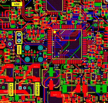
Figure 1. Example of a 4-layer board containing varying trace widths and types
The thicker traces have been optimized for current carrying capacity and are used for peripherals or power-related functions that demand higher power, such as fans, motors, and general power delivery to lower level components. And there’s even a differential signal (USB high speed) shown in the top-left section of the figure with specific spacing and width defined to meet 90-Ohm impedance requirements. Figure 2 shows a slightly denser board with 6 layers and a BGA (ball grid array) component requiring thinner traces.

Example of a 6-layer board containing a 256-pin BGA component with 5-mil trace widths
Let's walk through the process of calculating for a certain trace width for a power signal delivering current from one power component to a peripheral. In this example, we’ll be calculating the minimum trace width for a power-path used for a DC motor. The power-path starts at a fuse, travels through an H-bridge (a component used to manage power delivery across a DC’s motor windings), and ends at the motor’s connector. The average continuous max current demanded by the DC motor will be around 2 Amps.
Now, a PCB trace acts as a resistor and the longer and narrower the trace, the more resistance is added. If the trace isn’t properly defined, the high current could damage the trace and/or introduce significant voltage drop to the motor (resulting in a slower speed). NetC21_2 shown in Figure 3 is about 0.8” long and needs to carry 2 Amps max. If we assume some general things like a 1-ounce copper pour and ambient room-temperature during normal operation, we have what we need to calculate both the minimum trace width and expected voltage drop at that width.
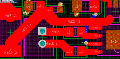
Example of optimized trace width for DC motor's power-path
The following is an equation used for trace area:
Area[mils²] = ( Current[Amps] / (k*( Temp_Rise[°C] )^b) )^(1/c) where following IPC guidelines for an external (or top/bottom) layer, k = 0.048, b = 0.44, c = 0.725. Note that the only variable we really need to plug in here is current.
And using this area in the following equation will give us the necessary width which tells us how wide our trace needs to be to carry the current without any potential issues:
Width[mils] = Area[mils^2]/(Thickness[oz]*1.378[mils/oz]) where 1.378 is associated with the standard 1 ounce pour thickness.
By plugging in 2 amps into the above calculation we get around 30 mils minimum for the trace.
But what this doesn’t tell us is what the voltage drop will be. This is a bit more involved as it requires a calculation of the trace’s resistance which can be calculated per the equation shown in Figure 4.
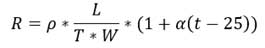
Figure 4. Formula for PCB trace resistance
In this formula, ρ = resistivity of copper, α = temperature coefficient of copper, T = trace thickness, W = trace width, L = trace length, and t = temperature. If all the associated values are plugged in for a 0.8inch long trace at 30mils width, we find that the trace resistance will be around 0.03? and will drop the voltage about 26mV which would be more than OK for the application. It’s helpful to know what impacts these values.
For digital designs with high speed communication, specific spacing and tuned lengths may be required to minimize cross-talk, coupling, and reflections. Some common applications for this are USB-based serial differential signals, and RAM-based parallel differential signals. Generally, USB 2.0 will require differential pair routing at speeds of 480Mbit/s (USB high speed class) or higher. This is partly because high-speed USB generally operates at a much lower voltage and differential, bringing the overall signal level closer to the noise floor.
There are three important things to consider when routing high speed USB lines: trace width, trace spacing, and trace length.
All are important but the most critical out of the three is making sure the two traces are matched as closely as possible in length. As a general rule of thumb, if the traces differ any more than 50 mils in length from each other (for high speed USB), it significantly increases risk of reflections which could result in poor communication. 90 Ohm matched impedance is a common specification for differential pair routing and to achieve this, the traces should be optimized in width and spacing.
Figure 5 shows an example of a differential pair routed for a high-speed USB interface, containing 12-mil wide traces at 15-mil spacing.
Figure 5. Differential routing for USB2.0 high speed
An interface for a memory-based component containing a parallel interface, such as DDR3-SDRAM, will be much more tightly constrained in terms of trace length. Most higher-end PCB design software will have length-tuning features that will optimize trace length to match all associated signals in a parallel bus. Figure 6 shows an example of a DDR3 layout with length-tuned traces.
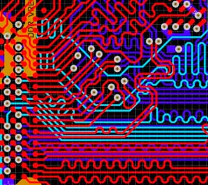
Figure 6. Example of length-tuned DDR3 memory traces
Some applications with noise-sensitive components such as wireless chips or antennas may require a little extra protection. Designing traces and planes with embedded ground vias can greatly help minimize coupling picked up by nearby traces or planes and also off-board signals that creep into the board edge.
Figure 7 shows an example of a Bluetooth module placed near the edge of a board with its antenna (labelled via silkscreen “ANT”) on the outside of a thick trace containing embedded vias connected to a ground plane. This helps isolate the antenna from the other on-board circuitry and planes.
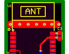
Figure 7. Bluetooth module with a ground-via embedded trace to help with noise suppression
Another method of this ground-via embedded trace (or polygon plane in this instance) could be used to protect the boards circuitry from outside, off-board wireless signals. Figure 8 shows a noise-sensitive PCB with a ground-via embedded plane along the perimeter of the board.
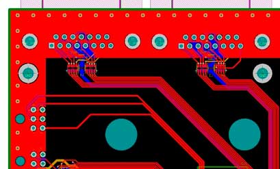
Figure 8. Ground plane with vias lining a sensitive PCB to protect against off-board interference
Many things drive trace characteristics in the PCB world so make sure to follow best practices when routing your next PCB and you’ll find that balance between PCB fab cost, circuit density, and overall performance.
If you’re looking for a quote for your next PCB application, connect with our team of experts to help you get exactly what you need at the right price. We specialize in PCB fabrication and PCB assembly conforming to intricate designs typical boardhouses can't manufacture or assemble.
Let us help you bring your design into reality.
PCB School
Standards like MIL-PRF-55110, MIL-PRF-50884, and MIL-PRF-31032 exist to enforce reliability, traceability, and performance in environments where failure isn't acceptable.
PCB School
Flying probe testing has been the golden standard of functional testing for low volume, prototype runs since the late 80s and 90s. It effectively flips the approach of the traditional in-circuit (ICT) bed-of-nails fixture test, where a custom-built frame with hundreds of spring-loaded pins contact test points simultaneously.
PCB School
Double-sided Ball Grid Array (BGA) assembly maximizes component density without increasing board size, enabling high-performance designs for applications ranging from smartphones and IoT devices to medical and industrial electronics.
PCB School
Managing strain during press-fit connector insertion is essential for high-density PCB reliability. Discover best practices and how San Francisco Circuits ensures reliable assembly for HDI, mil-spec, and medical applications.

PCB School
San Francisco Circuits covers the 8 types of PCB vias including blind, buried, microvias, through-hole, stacked, & thermal vias - what they are, how they work, & where they’re used in advanced PCB design.

PCB School
Discover why NIST 800-171 compliance is essential for PCB manufacturers. As a PCB buyer, learn how this cybersecurity framework safeguards your sensitive data & ensure you are engaged with a boardhouse that meets these requirements.
