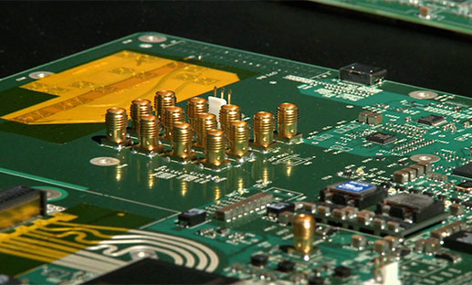
Printed circuit boards with Bluetooth technology can be problematic with interference, lost data and poor signal integrity if certain precautions aren't taken. We'll outline many rules and guidelines to consider when choosing Bluetooth technology for a given application and, more specifically, designing it into a circuit board.
A variety of applications utilize Bluetooth, including:
Each application incorporates the same common Bluetooth technology, but utilizes it differently and depending on the connection type, it’s up to the design engineer to incorporate basic principles to optimize signal integrity and overall device effectiveness.
Bluetooth is not a very fast wireless choice when compared to Wi-Fi, however it is getting faster. It also doesn’t do well through walls and other nearby obstructions and has a poor range.
It is still a good choice, despite being a work-in-progress (5.0 is the most recent update and is a decent improvement over 4.2). For the most part, it is a fairly low-power, reliable, secure, widely supported option that can easily be implemented on a wide range of small peripherals.
Bluetooth has been around for 20+ years and is still evolving and although it’s improved in speed, power, range, security and other attributes over the years, it still seems to have some of the same issues since its conception in the mid-90’s, including its susceptibility to signal interference.
So what can be done from a PCB design standpoint to optimize signal integrity, minimize interference and lost data packets?
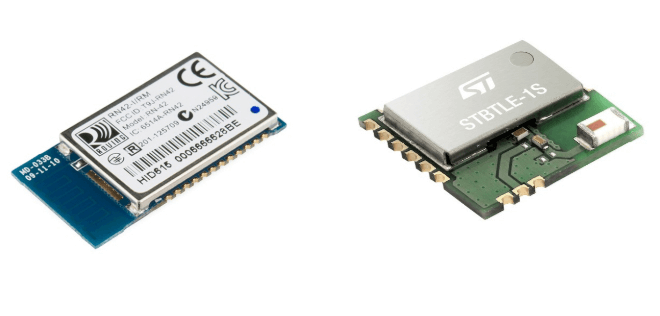
1. If you’re incorporating Bluetooth into a product and are limited on resources, consider using a pre-certified, fully contained module to help accelerate development and time to market. It may drive cost a little in the end but will usually prevent several headaches that can arise from antenna placement/design and EMI susceptibility.
There are several reasonably priced certified modules in the market today and most incorporate a small ARM processor, such as the RN4020 or RN4870 from Microchip, or the BT121 or BGM113 from Silicon Labs. Having the processor on-board gives it more flexibility and power, such as controlling simple peripherals via GPIO, SPI, I2C, PWM and so on, in addition to its Bluetooth stack.
2. Make sure you’re choosing an appropriate Bluetooth device for the application and that the antenna has also been appropriately sized and tuned.
If you’re going for a simple beacon application where you only need to advertise location or data in short spurts/intervals, then a low-power (Bluetooth Low Energy or BLE), cost-effective solution with minimal features and peripherals could be used to save on-board real estate and end cost.
If you’re looking for more of a higher throughput, audio-streaming or data-exchanging Bluetooth application, then you may need something that has a bit more Tx power, higher Rx sensitivity and a faster data-rate (although slowing down the data rate can typically help with minimizing dropped packets).
If you’re looking for a sort of all-in-one chip, consider using the chipsets containing powerful or secondary processors that include available UART, SPI, I2C, PWM, ADC, DAC and GPIO pins.
If you’re working on something heavily dependent on an RSSI reading, make sure it has enough dB resolution on its RSSI monitor.
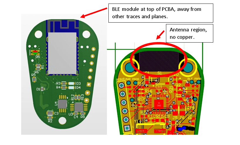
3. When designing in a Bluetooth chipset or module, keep the antenna region completely free from nearby copper signals or components carrying significant amounts of energy (especially power paths that are switched such as boost or buck converters).
This also includes keeping the area (and board layers) free of planes and polygon pours. Most Bluetooth chipset manufacturers will provide layout guidelines that should be followed closely during PCB design. If you’re manually laying out the antenna area, use a ground plane as appropriate to keep a good bandwidth at the input and make sure to build in enough room for tuning elements (a ground plane is required for printed and ceramic antennas).
Use ground stitching vias to prevent unwanted radiation from the PCB edge as it could penetrate nearby Bluetooth signals. If you can, try to make the board shape optimized to the Bluetooth device and where it’s antenna is, keeping it on the edge and far away from nearby components and signals. If using analog-based signals such as Audio, make sure that the analog and digital ground planes are separated.
And it’s always a good idea to shield the electronics (not the antenna of course) to prevent cross-coupling and minimize noise picked up.
4. Make sure that the rail supplying power to the Bluetooth module or chip is clean and use bypass (1.0 uF) and decoupling capacitors (0.1uF and 10nF) where needed. Also feel free to use ferrite beads on the power rail entering the Bluetooth area of the board to reject high frequency noise.
5. If you’re designing the antenna area, make sure you have the proper equipment (such as a network analyzer) to analyze and tune the matching network, or consider sending the design to a 3rd party RF test lab.
6. There are a wide variety of things that can cause obstruction or de-tuning during a Bluetooth connection, including nearby water (humans too… we’re made mostly of water), metallized objects, smart phones/tablets, computers, devices operating on the same ISM band such as microwave ovens or WLAN technologies, power sources, wireless RF video, office lighting and home phones.
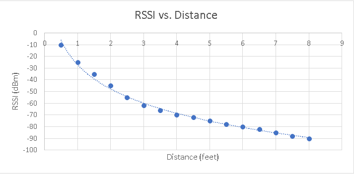
It’s hugely susceptible to signal loss even when paired at close distance (1-2 meters). If there is higher risk of these kinds of things impacting signal quality, then choose a higher power device and operate at a slower speed to minimize packet drop. Or if the electronics are inside of an enclosure, make sure that the metallized materials are minimized and far away from the BLE module. The relationship between Bluetooth signal strength and distance is not a linear relationship. In fact, it’s very non-linear and somewhat unpredictable based on the surrounding environment but does follow a general pattern (shown below).
Whether you’re designing a small, simple Beacon module or a data-streaming, power hungry Bluetooth hub, following these considerations could save you tons of headaches during the test/implementation stage of design.
With the expansion of Bluetooth PCB assembly, it’s an exciting time to incorporate wireless communication and control into products, and the future will only bring smaller, faster, cheaper and stronger Bluetooth components.
At San Francisco Circuits, we’re excited to help bring these new concepts into reality. Partnering with an experienced PCB manufacturing and PCB assembly provider with engineers that have long-standing relationships with component suppliers is crucial to the success of your next Bluetooth PCB fabrication and assembly needs.

PCB School
Standards like MIL-PRF-55110, MIL-PRF-50884, and MIL-PRF-31032 exist to enforce reliability, traceability, and performance in environments where failure isn't acceptable.
PCB School
Flying probe testing has been the golden standard of functional testing for low volume, prototype runs since the late 80s and 90s. It effectively flips the approach of the traditional in-circuit (ICT) bed-of-nails fixture test, where a custom-built frame with hundreds of spring-loaded pins contact test points simultaneously.
PCB School
Double-sided Ball Grid Array (BGA) assembly maximizes component density without increasing board size, enabling high-performance designs for applications ranging from smartphones and IoT devices to medical and industrial electronics.
PCB School
Managing strain during press-fit connector insertion is essential for high-density PCB reliability. Discover best practices and how San Francisco Circuits ensures reliable assembly for HDI, mil-spec, and medical applications.

PCB School
San Francisco Circuits covers the 8 types of PCB vias including blind, buried, microvias, through-hole, stacked, & thermal vias - what they are, how they work, & where they’re used in advanced PCB design.

PCB School
Discover why NIST 800-171 compliance is essential for PCB manufacturers. As a PCB buyer, learn how this cybersecurity framework safeguards your sensitive data & ensure you are engaged with a boardhouse that meets these requirements.
