PCB design: you need a CAD program for your project, but which is best?
There are already tons of articles like this available - and they’ll all bore you to death with the same mundane details (with the exception of a select few).
Our ultimate PCB design software comparison guide will crush all those articles.
Here’s why:
We’re going to run through a step-by-step tutorial of the same design to show how each critical feature grades out in the top PCB programs available.
Our unique guide begins by diving into a comprehensive comparison of the top 6 PCB design tools. And our tutorial will compare the best 3 (in our humble opinions).
There are several programs available that range from simple and intuitive to highly sophisticated.
They range from free or inexpensive to high-end/premium.
They come feature-less or feature-heavy.
All of the tools are different and unique in their own way. Ultimately, your needs and preferences should drive what CAD program you use. This guide is structured to help you decide which is optimal or explore alternatives.
It’s important to establish the criteria we’re using - which is, inevitably, subjective.
We also have biases for software that we’re extremely comfortable with compared to programs that we have had very little work with.
We really like this excerpt from Mathieu Stephan’s (AKA limpkin) excellent Altium vs. Cadence article to encompass our primary grading criteria:
“A PCB routing software should be easy to use...To define that subjective criteria, I'd like to propose here a simple 'easiness measurement metric' defined as number of clicks + number of keystrokes + mouse moving distance to perform a given function. Why? Well because a good portion of the time you spend routing your PCB (time is money) is the time taken to perform simple actions. When you have to click 5 times, move the mouse 5cm to the right and 4cm to the left to do a simple thing, and you have to do this simple thing one hundred times on your PCB... it can get pretty long and frustrating.”
In addition to Mr. Stephan’s easiness metric, the software should be a standard and widely used platform in the industry. This is important for team collaboration when the engineer’s skills are scaled to larger, wide-spread applications.
Finally, we consider the various feature sets and which programs are better for which applications. You’ll find that most programs have all the features you’re looking for, so the ease-of-use factor is most strongly considered.
Keep in mind that everyone will have a different preference so our opinions may not align with your needs and ultimate favorite.
It was pointed out to us, quite accurately, that it's important to note the program versions and review dates to provide some context to the date this article is being read. New features, fixes or changes may have been released that weren't available at the time of our review.
The dates we reviewed the software are found below:
DipTrace: September 2016, version 3.0
Eagle: September 2016
KiCAD: December 2017, version 4.0.7
OrCAD: September 2016, version 17.2
PADS: September 2016
Altium Designer: September 2016, version 16
Whichever PCB design software you select, reference our PCB School for additional electronic design tips:
And, when your design is ready for a prototype or production run, get in touch with us at San Francisco Circuits to bridge your concept with reality.
Successfully taking a complex PCB design from layout to PCB assembly is the core value that comes from partnering with San Francisco Circuits for your next project - from flex PCB to bare circuit boards, we are your one-stop shop for advanced printed circuit technologies.
The table below summarizes the key points of each program and a basic grade of each critical feature.
| Category/Criteria | DipTrace | Eagle | KiCAD | OrCAD | PADS | Altium | Scale |
|---|---|---|---|---|---|---|---|
| Basics | |||||||
| Ideal for (hobbyists, professionals, everyone) | hobbyists | hobbyists | hobbyists | professionals | professionals | professionals | |
| Price Range* | Free | Free | Free | $1,500 | $5,000 | $7,000 | |
| Learning Curve | A | B | C | D | D | C |
Grade: A – F |
| Support/Help/Tutorials | B | A | B | C | B | B |
Grade: A – F |
| User Interface/Navigation | B | B | C | D | F | A |
Grade: A – F |
| Personalization Options | D | C | A | D | B | B |
Grade: A – F |
| Category/Criteria | DipTrace | Eagle | KiCAD | OrCAD | PADS | Altium | Scale |
| Schematic Editor | |||||||
| Placing and editing components | B | B | C | B | C | A |
Grade: A – F |
| Placing and editing electrical objects (wire, ports, etc.) | B | C | C | B | B | A |
Grade: A – F |
| Placing and editing graphical objects | C | C | B | B | B | B |
Grade: A – F |
| Annotation | C | B | A | B | B | B |
Grade: A – F |
| Overall Schematic Editor | C | C | B | B | B | B |
Grade: A – F |
| Category/Criteria | DipTrace | Eagle | KiCAD | OrCAD | PADS | Altium | Scale |
| Schematic Library Editor | |||||||
| Adding pins and component shape | B | B | A | B | B | A |
Grade: A – F |
| Defining connection type and descriptions | B | B | B | C | C | A |
Grade: A – F |
| Multi-part schematic component | B | C | C | C | C | B |
Grade: A – F |
| Integration with PCB footprint and PCB library | C | C | D | D | C | A |
Grade: A – F |
| Adding simulation properties | N/A | N/A | D | B | A | C |
Grade: A – F |
| Overall Schematic Library Editor | B | C | C | C | C | A |
Grade: A – F |
| Category/Criteria | DipTrace | Eagle | KiCAD | OrCAD | PADS | Altium | Scale |
| PCB Library Editor | |||||||
| Defining and placing pads | B | C | B | B | B | A |
Grade: A – F |
| Custom/irregular shapes | B | B | C | B | B | B |
Grade: A – F |
| 3D visual | A | D | B | C | D | A |
Grade: A – F |
| Defining other layers around footprint (silkscreen, keepout, solder mask, courtyard, etc.) | B | C | C | A | B | A |
Grade: A – F |
| Overall PCB Library Editor | B | C | C | B | B | A |
Grade: A – F |
| Category/Criteria | DipTrace | Eagle | KiCAD | OrCAD | PADS | Altium | Scale |
| Other Criteria | |||||||
| Database Management | N/A | N/A | B | B | C | B |
Grade: A – F |
| PCB Routing | B | C | A | C | C | B |
Grade: A – F |
| Net Management | B | B | B | A | B | B |
Grade: A – F |
| 3D Visualization | A | D | B | C | D | A |
Grade: A – F |
| Error Debugging | B | C | A | B | B | A |
Grade: A – F |
| RF Design | C | C | B | B | B | B |
Grade: A – F |
| FPGA Design | N/A | N/A | N/A | C | A | C |
Grade: A – F |
| File Generation | A | A | B | C | B | A |
Grade: A – F |
* These costs vary widely so we quoted a simple, single license that allows for small to medium size/complexity designs with no special add-ons or features. Does not include maintenance/renewal discounts but just first year purchase.
All grades are for basic, comparable feature sets, meaning that a PCB program will not score any higher because it has more features available, and the ones they have in common are the focus of the grade.
DipTrace is one of the most affordable and simple programs available, ideal for hobbyists but less suitable for professionals or complex schematics.
If you’re looking for something basic to get a 2-4 layer board made and some thru-hole or bulky surface mount components or are just starting out, DipTrace is a good start. It’s very intuitive with a low learning curve, but is limited in ability.
DipTrace has a free version which is limited by 300 max pins and 2 layers, which is fine for simple projects.
More complex designs will likely need to upgrade to the unlimited version priced at $895.
DipTrace features include:

The DipTrace Verdict:
Overall, DipTrace is pretty good for smaller, simpler boards and is very easy to learn. It’s a good starter CAD that will teach you board design skills that can be applied to more advanced CAD programs.
For anything more than just whipping up simple PCBs for hobby/prototype projects, you’ll need to upgrade or look for something with more capabilities.
John Teel, a prominent electrical engineer and founder of Predictable Designs, has first-rate review of DipTrace, Altium, Eagle and OrCAD. To illustrate how much personal preference factors in the software, John ultimately favors DipTrace over the other programs and provides a solid write-up of the platform.
John also shared a point of view with us regarding our conclusion that we feel is important to share:
“I disagree with your summary that DipTrace is only good for simple designs. I have done some very complicated designs using DipTrace. This includes designs using high-pin count application processors, BGA parts, and products with as many as 5 different kinds of wireless radios. With the full version there is no limit on the pin count. My biggest complaint about DipTrace is that it's not very common. If you need to work with other PCB designers then something like Altium or Eagle is a better choice.”
He has a point and our lack of familiarity with DipTrace surely played a part in our final verdict.
If you’re looking for something a little more complete but still low-cost and easy to use, Eagle CAD is a good choice.
It’s one of the most popular CAD programs used and has tons of support from various forums and online communities. There’s also an abundance of good YouTube videos for tutorials.
The interface is still a bit clunky compared to some of the more high-end programs but it does have quite a few useful features.
Eagle stands for Easy, Applicable, Graphical, Layout, Editor. And it’s just that.
It comes in several flavors: Freeware, Eagle Learn, Eagle Make, and Eagle Business, and all with different tiers of layout, schematics, autorouter, and so on.
You can pay up to $1,640 for a single license but you may not necessarily need all of its features.
$410 will buy you 99 schematic sheets, 6 layers, and a 160mmx100mm routing area which isn’t too bad.
$820 will get you 999 sheets, 16 layers, and 4mx4m routing area, which is more than enough for most advanced PCB projects.
Eagle CAD features include:
A schematic editor with many typical features such as:
It also includes several other features such as:
The layout editor includes standout features like:
The Eagle CAD Verdict:
The best thing about Eagle is the online support. It’s a little more complex than starter CAD packages, like DipTrace, but nearly every issue can be solved through the vast support system.
And it’s also one of the more widely used board design programs, containing several thousands of pre-made libraries and used for the following popular platforms:
SparkFun Electronics, Dangerous Prototypes, Adafruit, and Element14, all popular DIY and distributing electronics stores use Eagle CAD religiously and almost always have designs available for editing.
Overall, it’s a good middle-of-the-road program for most beginner to advanced PCB projects out there for a decent price with a learning curve that isn’t overwhelming. Ultimately, we prefer DipTrace over Eagle CAD.
Two programs that are more used in the industry and not so much for hobbyists are OrCAD and PADS, which we cover in the next 2 sections.
They’re both fairly similar to each other and have several more features and capabilities than Eagle, but do come at a higher cost.
Another decent middle-of-the-road program for most beginners and hobbyists trying to save some $$ during PCB and schematic capture is KiCAD. It’s completely free and is maintained by volunteers and paid contributors (which more recently have been CERN-based organizations/programs), and it has improved greatly over the last few years. It is also widely accessible as it exists on almost every major platform out there (similar to Eagle) including Linux, Windows, and Mac OS X.
Its schematic capture (or Eeschema) works similar to Eagle and most other CAD programs and contains a few notable tools:
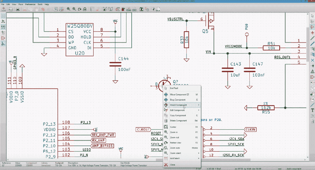
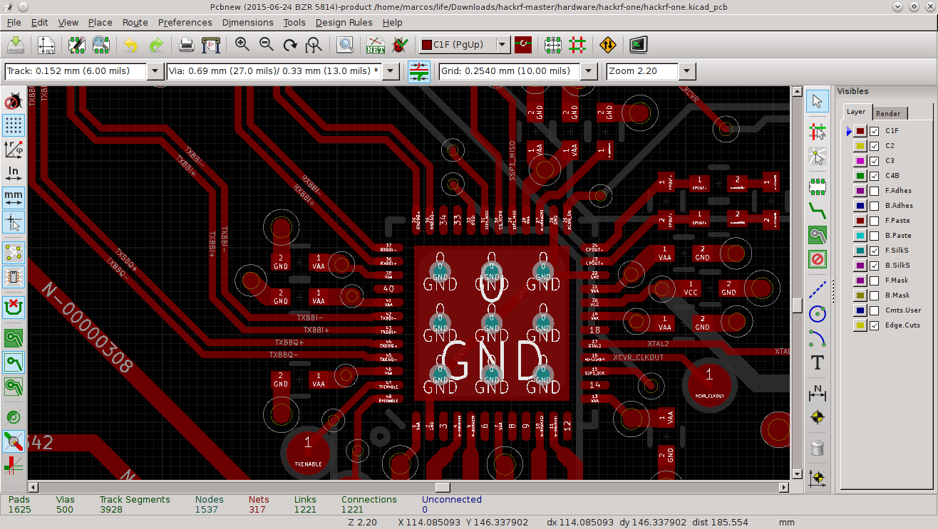
However, the schematic environment is separate from the PCB environment, which is called “PcbNew.” It requires a netlist to be exported and loaded in the PcbNew program, sort of like OrCAD, which seems a bit clunky. However, PcbNew has some pretty amazing features for free PCB layout software.
For one, it has a ton of hotkeys which are all completely configurable via the hotkey editor. At first, this can make things very confusing but, like most software programs containing hotkeys, they become more and more convenient the more you use them especially on heavily used tasks, such as placing vias and tracks. This makes up for the seemingly older looking, less-intuitive UI.
You also have several options when routing, including push/shove conforming to saved design constraints/rules, automatic re-routing around obstacles, length tuning and matched differential pairs for high speed applications, and making post-routing tweaks such as dragging or shortening traces.
KiCAD has a feature called CvPCB which works sort of like Altium Vault, in which it utilizes an online network of library parts, mostly in Github, managed by the large community of KiCAD users. With 133 repositories (at the time of this writing – January 2018) and tons of libraries to choose from, it allows for easy quick access to common parts and saves time developing (and makes learning a bit easier too).
However, the library editor itself isn’t terribly intuitive and is a bit more laborious or manual than something such as the component wizard offered by Altium.
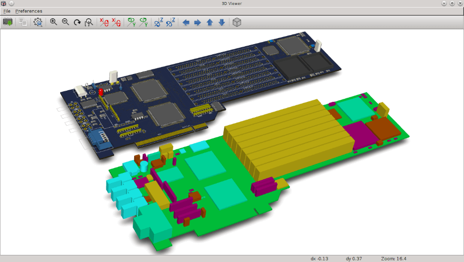
PcbNew also has a pretty decent 3D viewer and modeler. The PCB editor viewer itself is a little archaic with different font types/sizes and a crude layer/color system, but the ability to import and export STEP models makes things a lot easier when working with mechanical teams or certain mechanical features.
In general, KiCAD offers some fairly powerful and advanced features for a cost point of $0, but it isn’t the easiest CAD software to use (at first at least), and takes some warming up to. A lot of people transition from Eagle to KiCAD once they are able to take advantage of the more advanced features given its price point, but it requires a bit of an open-mind, patience, and even some community involvement.
OrCAD comes in a variety of tiers, outlined in this chart:
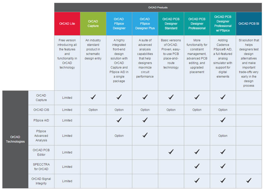
OrCAD Lite allows you to be able to experiment with a little of everything and some limited features for free.
It’s easy to upgrade after you have it installed to something a little more standard, such as Designer Standard which includes both schematic and PCB editing (available for around $1500/year).
Note that OrCAD and Allegro are being treated as essentially the same product for the purpose of this comparison. OrCAD is pretty much a scaled-down version of Allegro.
OrCAD features include:
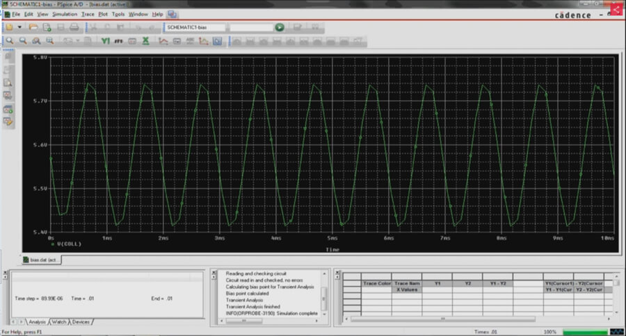
One major thing that separates OrCAD from the lower end CAD packages is the PSpice add-ons that allow full circuit simulation.
It does have quite a learning curve but if you have it at your disposal, it can save you a ton of time and frustration on some of the more advanced mixed signal designs. There are even entire courses in college focused on just learning how to use this one feature.
OrCAD CIS allows you to integrate component information in a database, something that is useful when working in a bigger team with an accelerated design cycle.
Finally, there is SPECCTRA which is probably the best auto-routing software out there. Again, we’re not huge fans of auto-routing but SPECCTRA does work very well.
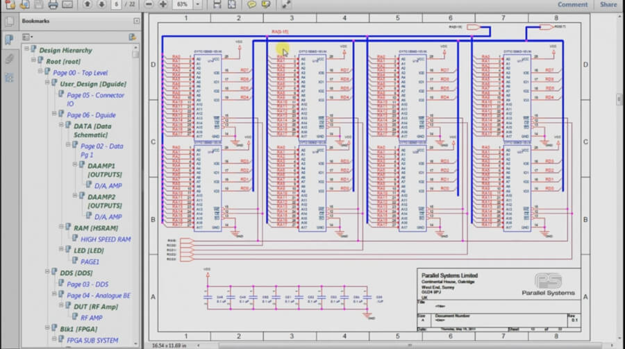
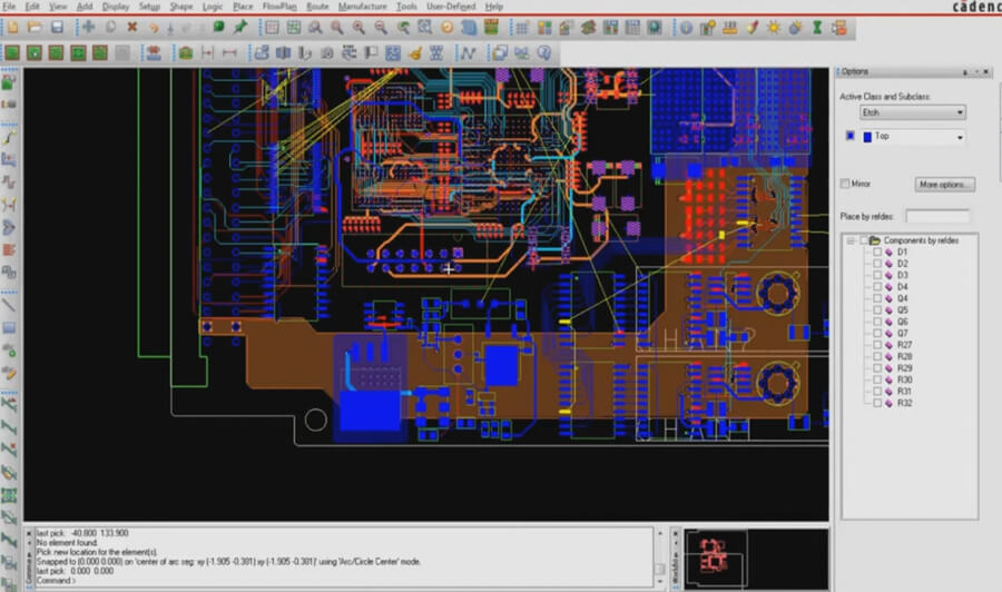
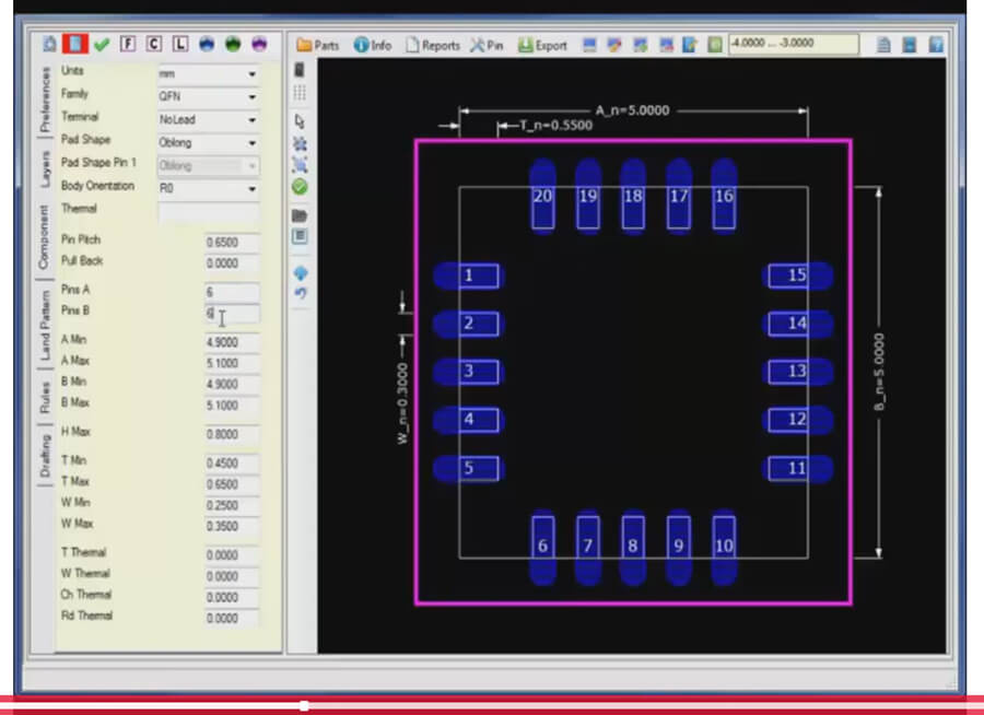
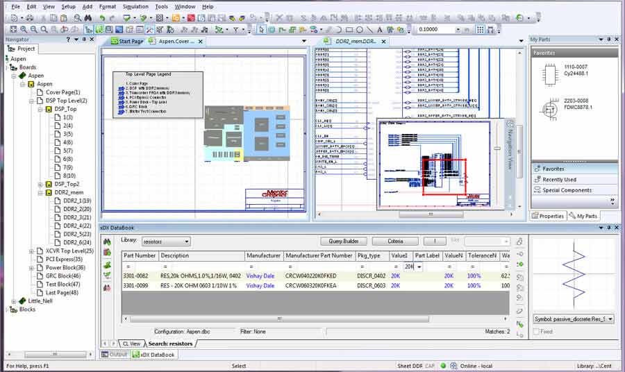
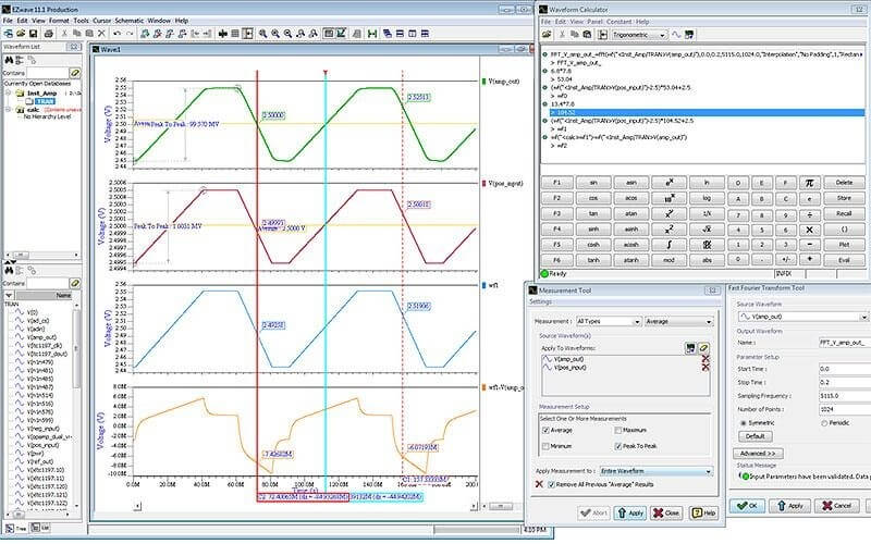
Let’s take a look at some screenshots of the schematic editor, PCB editor, library builder, and PSpice simulator.
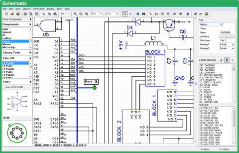
OrCAD Screenshots:
The OrCAD Verdict:
One drawback of OrCAD is how it splits up every feature into standalone applications. Each feature has its own program; nothing is integrated.
This is a little annoying and you’ll find yourself toggling between several windows when developing 1 board.
Its 3D rendering isn’t the greatest (compared to Altium), but it works. OrCAD is very powerful and an industry standard, but it’s just a little outdated in our opinion.
Like the other CAD packages, PADS comes in a few different package levels but the Standard edition should contain most of the features needed.
It’s more expensive than OrCAD but it does work very well.
One bonus about PADS is it has translators (like Altium) that imports PCB projects from other programs such as OrCAD or Altium. This is extremely useful if previous products were designed using different board packages and need revising.
PADS features include:
Beyond the basics (schematic creation, library/part management, design rule verification, PCB design), PADS also has wizards for walking the designer through creating parts and a 3D tool that allows import/export of STEP files.
For anything high speed related we recommend PADS over OrCAD as it has some great RF and microwave design features. It allows for automated via stitching in and around traces/pads, importing complex RF components/shapes, shielding, chamfering trace corners, and more.
The Standard Plus Edition includes some additional high speed design constraints and features, such as differential pairs, matched length routing, and signal integrity analysis. It also includes analog simulation that blows OrCAD out of the water, as well as some other great features like thermal analysis.
Finally, the Professional edition includes all that plus additional design guidelines for fabrication, drawings, and panelizing. There are even some additional add-ons that can be used for FPGA design, enhanced RF and high speed design features, access to millions of 3D models, and more.
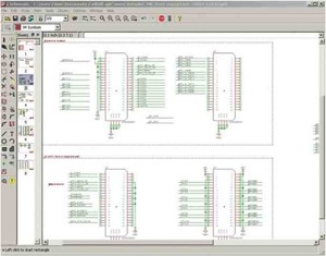
PADS Screenshots (from their website):
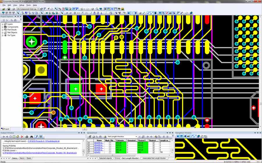
The PADS Verdict:
As previously stated, PADS is superior to OrCAD for high-speed, RF and microwave technology design.
Given all these features and capabilities, it does have a bit of a learning curve.
There are several other higher-end board design programs out there but we’ll go into one that’s becoming more and more popular throughout the design community: Altium Designer.
It’s mainly used by industry professionals due to its feature set and higher learning curve but is, in our opinion, the best option for professionals anywhere in the industry.
What makes Altium so great are all the little things - the little nuances you get from other CAD packages that simply don’t exist.
It’s certainly not the most powerful program and doesn’t have a great FPGA design feature (it does have an entire section of this but it’s a little weak in comparison to the other high end packages).
It could use a better auto-router (a feature that should not be extensively leaned on) but makes up for it in the feedback-driven improvements made over the last several years, making it one of the most user friendly and efficient PCB CAD programs on the market.
The schematic design is pretty similar to most other packages but the PCB editor is where it excels.
Altium Designer features include:
The incremental improvements made on these kinds of design features for daily use add up and allow the designer to have a much quicker design experience.
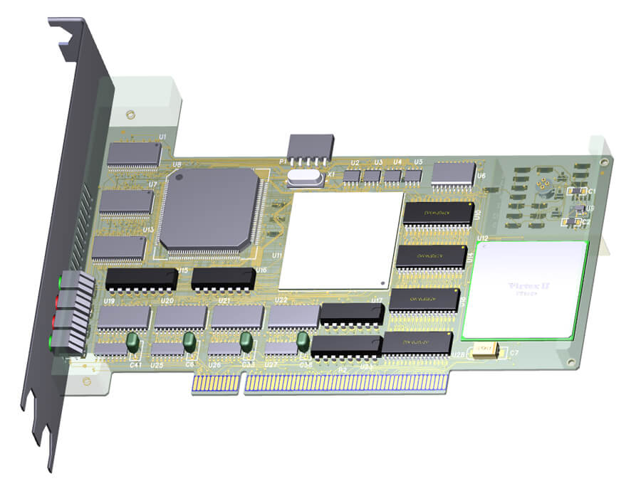
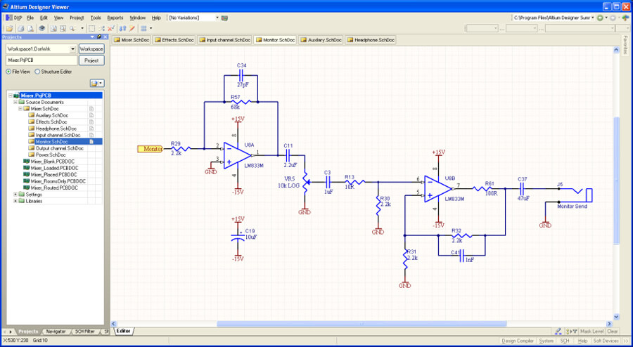
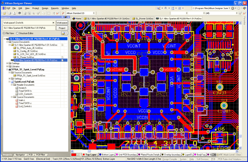
Altium Screenshots:
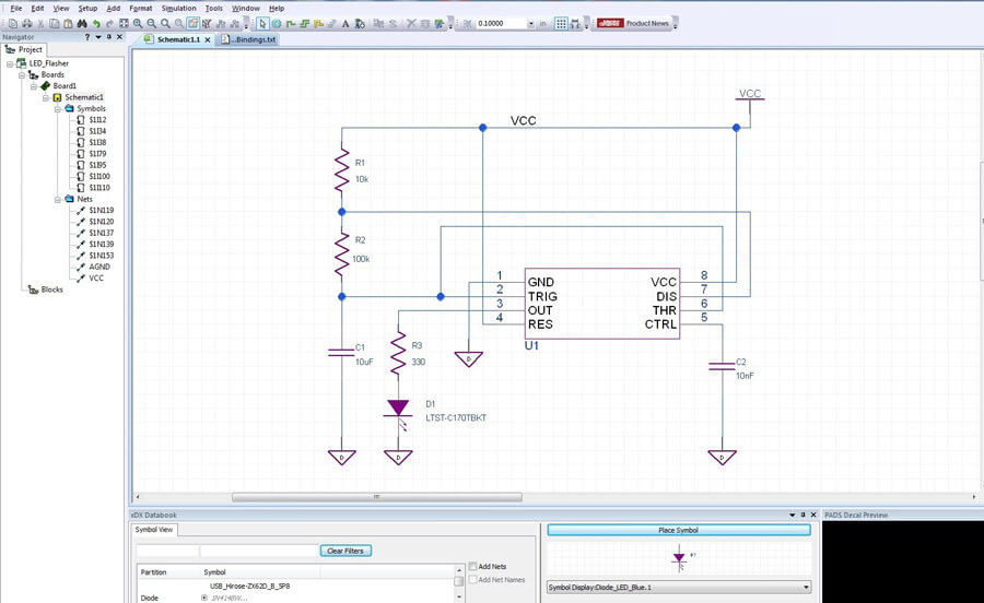
Our bird’s eye view of the most popular CAD programs may not provide a thorough enough comparison, so we’ve taken the top 3 PCB design programs and created the same PCB project in each one to show how each program grades out on an even playing field.
We’ll do a simple project:
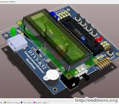
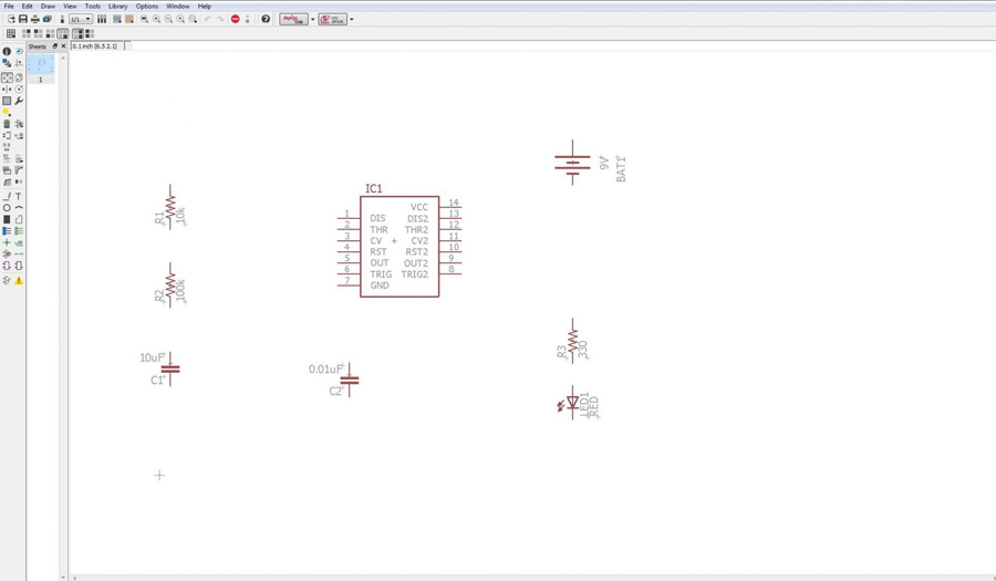
A 555 timer with an LED that contains 7 total parts.
This project will have enough component variety and traces to really highlight the differences between each CAD package.
Note that we won’t go into every single detail on building the design in each program but we will try and highlight some likes and dislikes as we go through it.
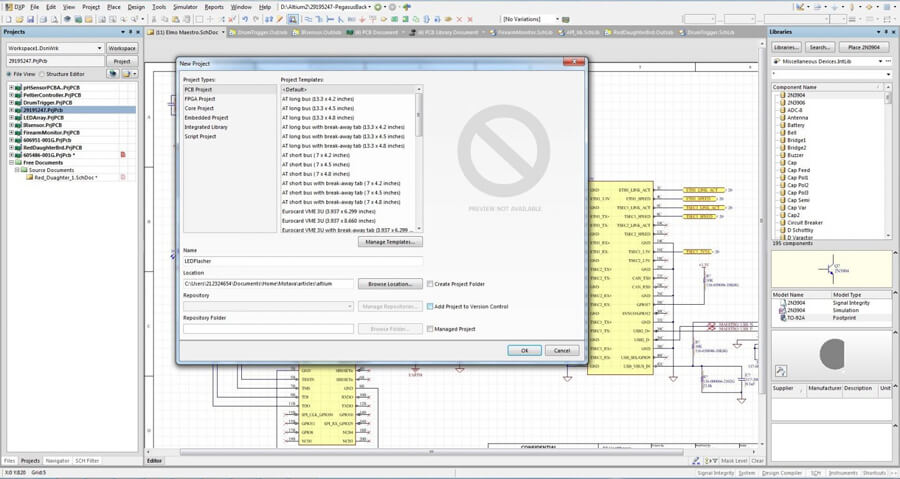
Creating a new project is very simple:
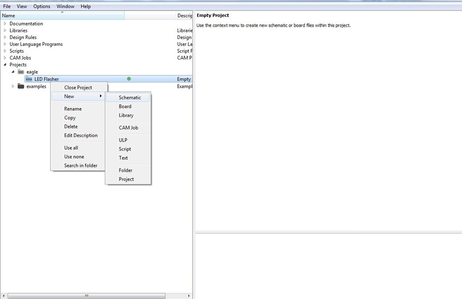
To begin, we’ll place the first part.
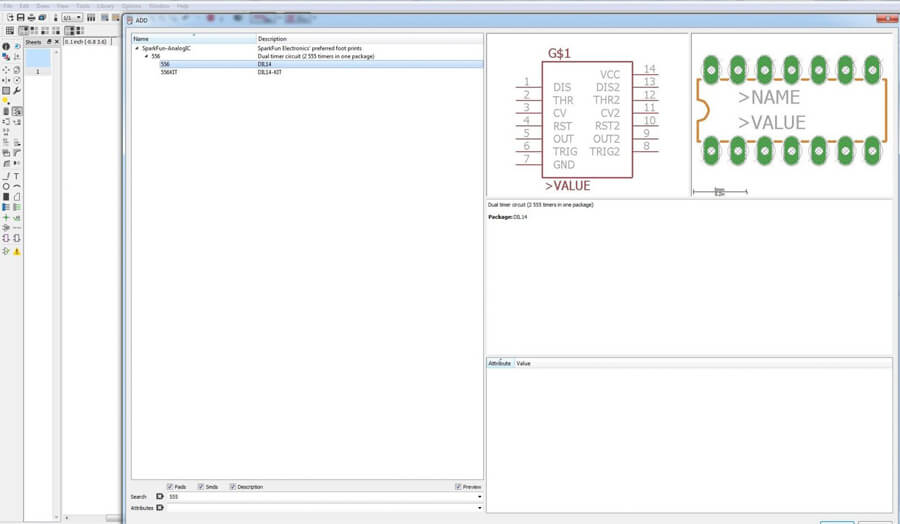
There are TONS of libraries out there for Eagle. Almost every manufacturer and some big DIY electronics sites have Eagle compatible libraries.
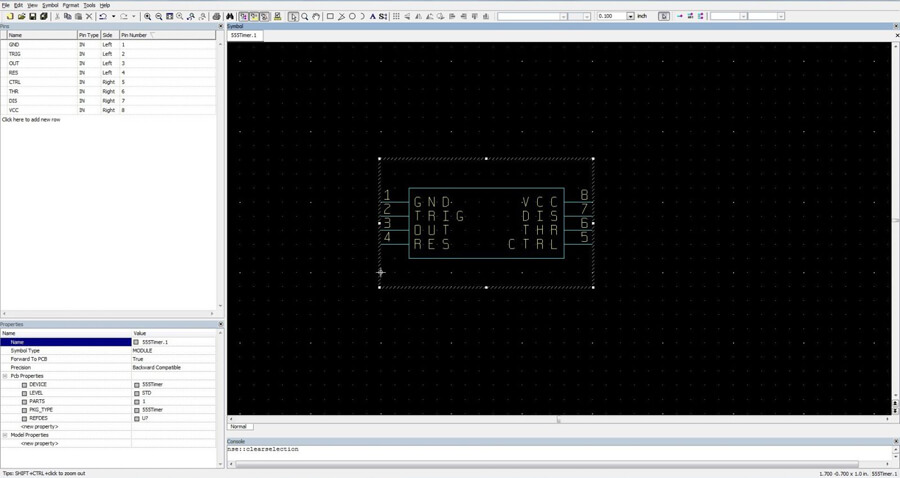
We added Sparkfun and since we need a 555 timer, we grabbed the dual 555 timer chip from the library and placed it in the schematic. It’s easily found by typing “555” in the search field.
A big pet peeve we found is with selecting parts in Eagle.
You can’t just click on the part. You, instead, need to look for the little crosshairs symbol (usually in the center of it) to move, rotate, or flip it.
You also need the “move” feature turned on, which is annoying to toggle back and forth between cursor select tools and such.
Now that the IC is on the schematic, we’ll look for some generic resistors, capacitors, and an LED in the library, and populate the schematic with everything needed.
We’ll then open up the properties for each and fill in the value. Another nuisance is to move text around, the designer has to “smash” the part. This causes just another step involved in moving things around and organizing your schematic.
A nice shortcut as you’re populating the schematic is pressing ESC, which will pop up the library, and one can move on to the next part automatically.
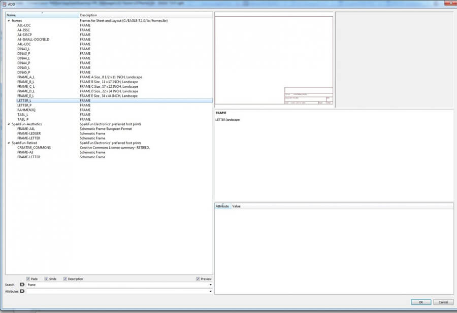
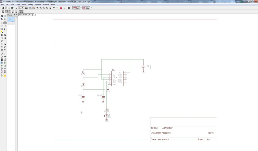
One other thing the schematic needs is a frame, which, if you have some templates in the library (again, we’re using Sparkfun), are extremely easy to add to the schematic.
It’s pretty basic but gets the job done.
Adding wire to the schematic is a little basic and pretty straightforward. There aren’t any fancy features here, basically just connecting A to B. Right-clicking does toggle through a few different routing options, but that’s pretty much it.
An aspect we like about the wiring is that once a component has wire on it, it’s easy to drag around and fix wire (compared to some other CAD packages that require a bunch of clicks to get it to where you want).
Copying components isn’t just as simple as copy/paste.
The designer has to make sure the right cursor mode is on, which is a bit cumbersome when trying to put grounds everywhere in the schematic. The same goes for moving multiple parts; you have to be in the right mode (group).
Part Naming
It’s nice that Eagle automatically increments and names your reference designators as you go. When you copy and paste a resistor, it’ll increment it to the next one (like R2 after you already have an R1).
If you wanted to custom name things, you can do that too. There’s also a SHOW tool that allows one to verify connections across the schematic. This is a very good visual check that everything is as it should be before routing (not even the best Design Rule Checks will catch some of these misconnections).The PCB Layout
The PCB Layout
This part is really easy.
Hit “Switch to board” under the File menu when the Schematic is open and it’ll ask to create a new PCB file, then populate everything in there for you.
The PCB editor and Schematic editor are two different windows, a minor annoyance when compared to programs like Altium. After importing the design, the software will show your components in the PCB editor with the gold connection wires highlighting the nets.
Moving these components in a semi-routable manor and re-sizing the board shape leads to the picture below:
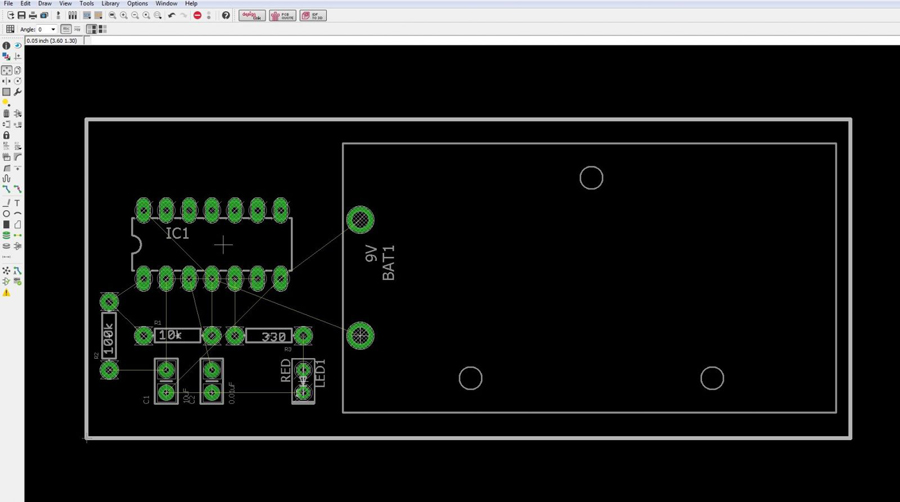
Moving around components in the PCB editor is pretty basic. Use the “move” tool to select and move components. One can also right-click while a component is highlighted to rotate and grid size can be adjusted as needed, which is all pretty straightforward.
Again, moving multiple components requires you to be on a different setting called “group tool” which is very annoying.
Routing
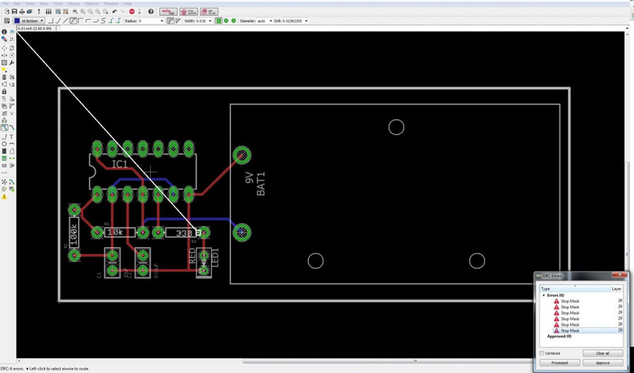
One thing we don’t like about the routing is it won’t provide real-time feedback on overlapping, shorting, etc. traces. It’ll only specify this when a DRC check is run.
Be conservative about the traces, or you’ll need to go back and correct mistakes after everything’s routed. Toggling between routing modes is easy, done simply by right-clicking.
Routing this simple design was really fast but for higher complexity designs, the routing features will limit you quite a bit.
There are a couple nice ways to make sure everything is routed. Hitting ratsnest will tell you whether or not you’re done with making the connections (in the lower left-hand corner). The DRC (like in most other CAD programs) will tell you in detail what needs to be corrected.
Eagle’s DRC is pretty bare minimum but it checks most things for you.
A few other things we won’t go into too much detail on are the polygon pours, silkscreen editing, and drawings.
They’re fairly limited features with not a whole lot to them. Also, one has the option of exporting the design to DXF, which is useful for mechanical teams, but the 3D viewer is pretty complicated to setup and operate.
Overall, this feature is not really worth the time needed to utilize.
Gerber generation is the last step, and it’s pretty simple with Eagle if you have a pre-made CAM file. Simply process the job and the files spit out into the current project directory.
The Verdict
Eagle’s great for simple projects or even middle-of-the-road ones if you have the patience and you’re on a tight budget. If you are able to pay for more advanced features and some added convenience, the next 2 programs will be better suited.
Now we’ll do this same walkthrough with PADS.
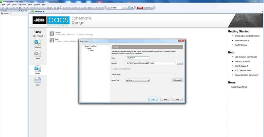
Creating a project (pointer to all PCB files) is pretty straightforward:
Unfortunately, just like OrCAD, there are separate windows for working in the schematic and PCB editor. It’s annoying to not have everything in the same window but PADS does make up for it with its intuitive interface.
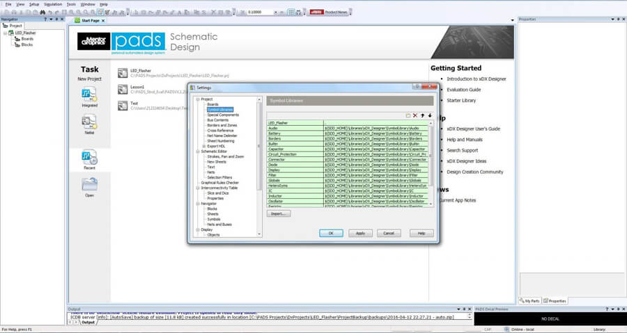
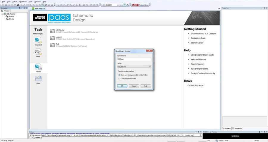
It comes standard with some library footprints already available but more can be added by hitting the “new library symbol” and force the library editor window to pop up (another editing window).
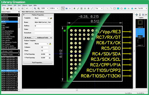
Let’s create the 555timer footprint.
In this designer’s opinion, the library editor interface is really not that intuitive.
Adding pins is a fairly slow process and the graphics could use some modernization (with some work you can define things the way you want for future use, but it does take time and doesn’t come as the default).
PADS does have all features needed to create library footprints but it’s just a little scattered and slow. No real hotkeys exist for this either.
Part Naming
Assigning pin numbers takes forever, users are required to click 3 times on each row under the pin number and then the program re-sorts, which threw us off every time.
The numbers then appear under the actual pin (who wants their pin number underneath the pin?!). We found we had to move the number above the pin every time. There’s also a symbol outline that needs adjusting, as well, when you’re resizing the component and adding pins.
These are minor inconveniences that slow the designer down when creating higher density footprints and lead to some frustration.
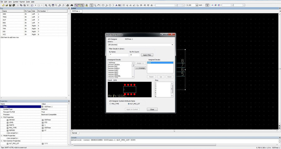
One thing that is nice about this library is how many pre-loaded footprints it comes with. Hitting “PADS decal browser” will display the thousands of pre-loaded footprints that can be filtered by number of pads and assigned to the current symbol.
When working in the schematic, a really nice detail (when first getting acquainted with the program) is the little tutorial videos that can be watched when hovering over the tools and icons.
They greatly help overcome the learning curve. PADS has pretty good help tools, in general, and the guide is very descriptive and easy to navigate.
However, during our test, it appeared that some of these links were broken or inactive.
Placing components into the schematic is pretty straightforward, and again, the default libraries come well stocked.
We were able to easily edit the capacitor value but for some reason the resistor value wasn’t able to be edited. Maybe it was an issue with the evaluation license we were using (which took forever to get installed and required a couple phone calls).
So we edited a different property (DEVICE) and had that displayed next to each resistor. But eventually we got all the components situated with their values and ready to wire up.
Moving text around components is a little clunky. The designer has to hold for a second or two and not drag the mouse. And if you have a ref des over a symbol, it becomes nearly impossible.
There are hotkeys for things like rotating components but they are unnecessarily challenging. Ctrl+Shift+R to rotate something, for example.
We also find the panning feature for the schematic to be underwhelming. This all seems a bit nit-picky but all of these minor frustrations really do add up.
The PCB Layout
When moving from the schematic to the PCB, the program asks if you want to automatically assign reference designators and creates a netlist for you. You can then open up the PADS Layout tool and import the netlist.
When we did this, we found that none of the schematic symbols had any PCB footprints associated with them (we assumed that, like normally pre-stocked library components, they did).
The Verdict
PADS is our least favorite PCB editing tool of the 3 outlined in this tutorial. It’s clunky and not very intuitive. We’re sure once you take trainings and spend several hours with it, you can get the hang of it but it may not be worth the trouble.
We’ll try not to sound too biased but walking through a simple project in Altium is like a breath of fresh air.
One thing about creating a project - we almost never do it this way as there are a ton of configuration options that are saved with the .PrjPcb file and we end up just copying and pasting the file, then renaming it.
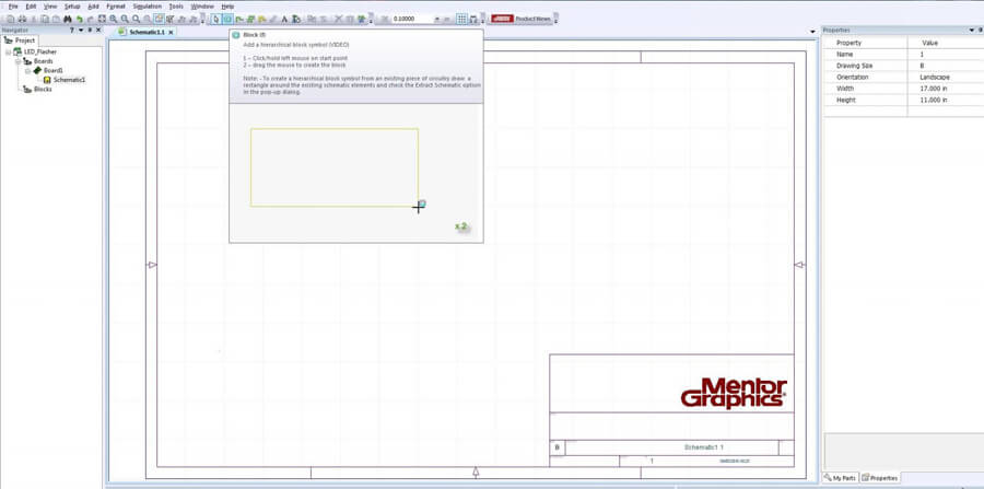
Adding a new schematic sheet can be done by looking over in the project tree, locating your current project, right clicking and choosing “add new to project”, then schematic.
You’ll see that you can add much more to the project this way, and that’s how you build your PCB file. It’s all pretty straightforward and all done and managed within the same main window.
Another great feature Altium has is how customizable the UI is. We like to have the library pane on the right showing the PCB footprint and 3D model associated with the component, making it easy to just drag and drop into the schematic. You can define what’s in your Projects view - we usually just have the project tree, library, and filter.
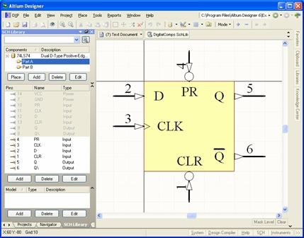
There are many pre-loaded, common schematic and PCB footprints to choose from. There is no 555 timer though, so let’s create our own.
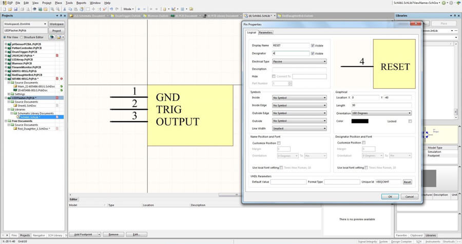
Same as adding the Schematic, just add a SchLib to the project and watch it fall underneath “libraries” inside your project.
The editor is fairly straightforward and has tons of hotkeys associated with it to make it easy when creating a component with several pins. Most ICs just have a rectangle and pins but if you needed to draw custom shapes, it’s fairly easy to do so.
We won’t go into the footprint editor because it’s fairly straightforward as well. It actually comes with a wizard that walks the user through several different types of packages and does all the spacing for you.
We ended up just grabbing an NE555 chip from an integrated library downloaded from the Altium website. It contains several common chips and we highly recommend it to anyone (it also contains several useful parameters about each component such as manufacturer part number and distributer). An integrated library basically combines the schematic library with the PCB library - pretty nifty.
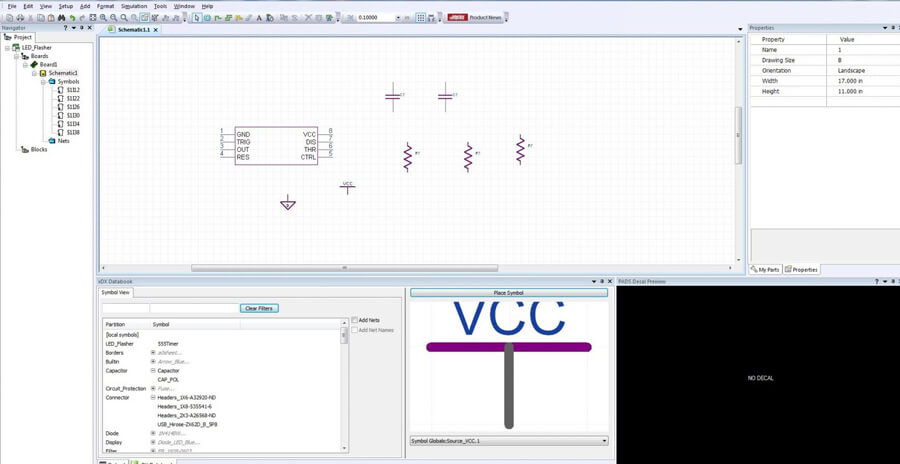
Looking through that same integrated library, we find the necessary resistors and capacitors needed to build the circuit. They all have the associated PCB footprints built in.
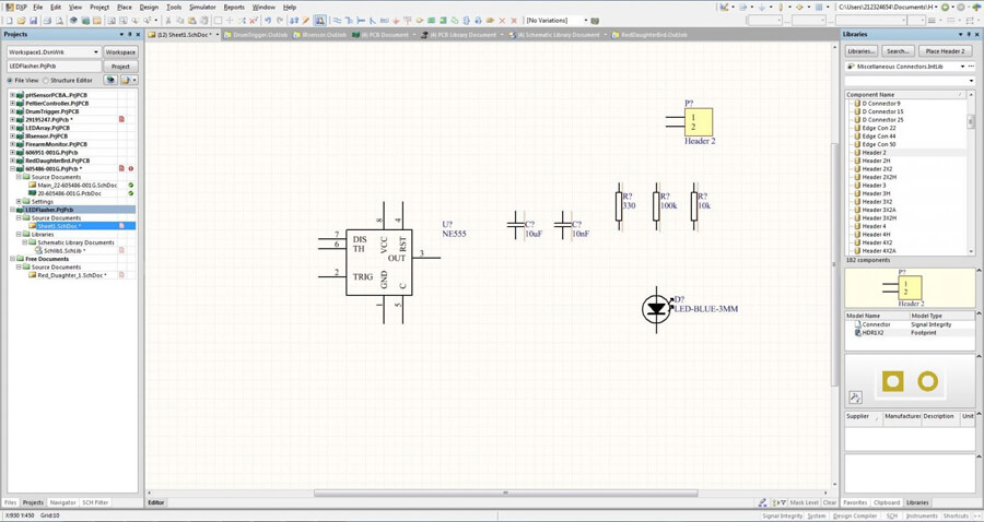
Moving things around and wiring them up is pretty straightforward and Altium has some nice toggling features to toggle between modes on the fly.
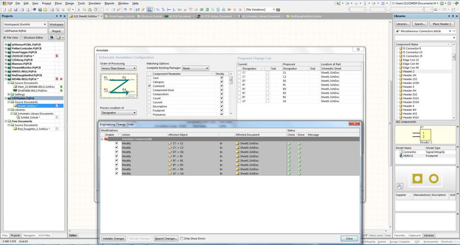
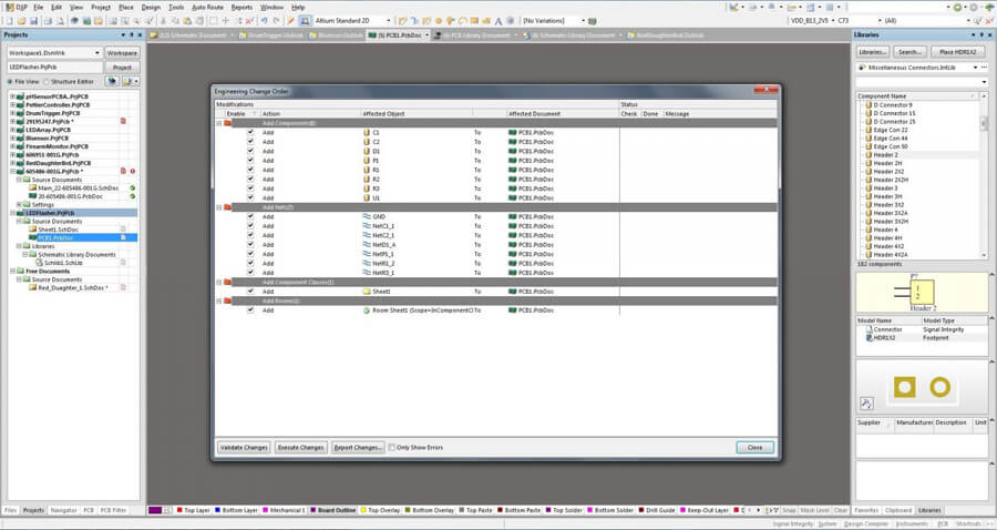
Resetting reference designators and re-annotating them is particularly easy and introduces you to one of Altium’s best features: the ability to outline all the changes in front of you, validate them and then execute.
It does this with an “ECO” process (generally stands for engineering change order) and it literally lists every single change you’re about to make to the design and displays whether it was successful or not. This may seem like overkill but when you’re moving around the design making changes, it’s a really nice visual check to make sure you’re changing what you want.
Part Naming
Annotating the schematic shows you how easy this really is.
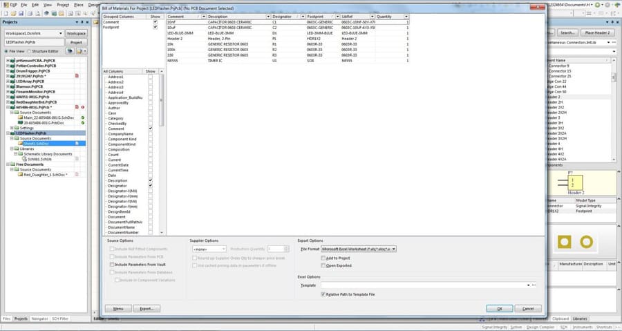
And now our schematic is wired and ready for PCB layout. One thing we recommend doing at this step is create the Bill of Materials (BOM). Another awesome feature of Altium is previewing and exporting the BOM to Excel.
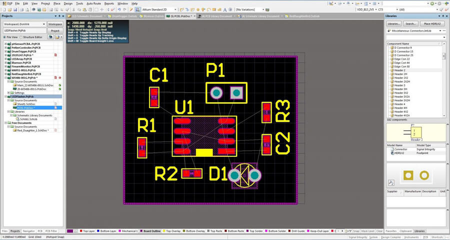
The PCB Layout
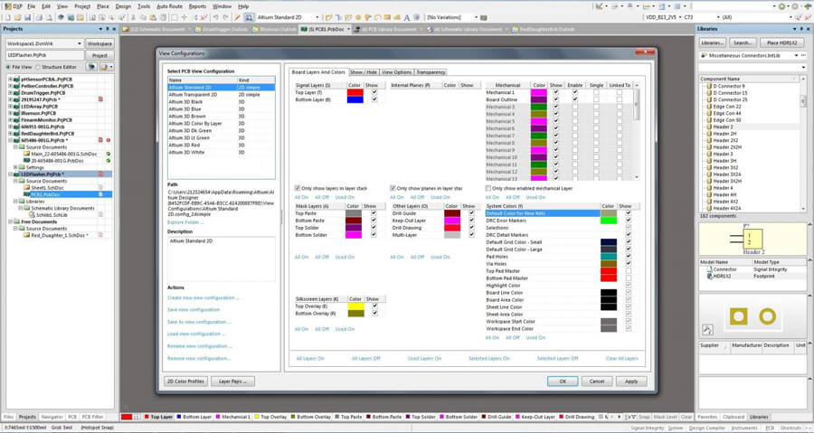
Now we have to add a PCB to the project. This is done the same way as the schematic and library. It comes with a bunch of standard layers that can be edited but custom layers can also be created for mechanical things, such as the board outline.
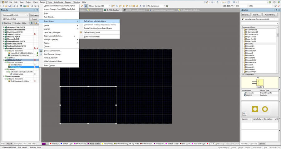
Defining the board shape based on a layer is pretty simple and allows you to create custom board shapes from imported DXF drawings. We just drew a rectangle for the simple PCB example.
When importing the schematics, you get to see every single thing through the ECO process, including the components, NETs, PCB footprints, classes and even the room.
Once everything is imported it shows up next to the PCB. Now is when the designer will want to change settings such as design constraints, routing preferences, grid size, active layers and more.
We won’t dive into that stuff as it does contain some learning curve but it goes quite fast after learning how. The desired preferences can also be saved and used in other projects.
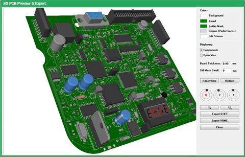
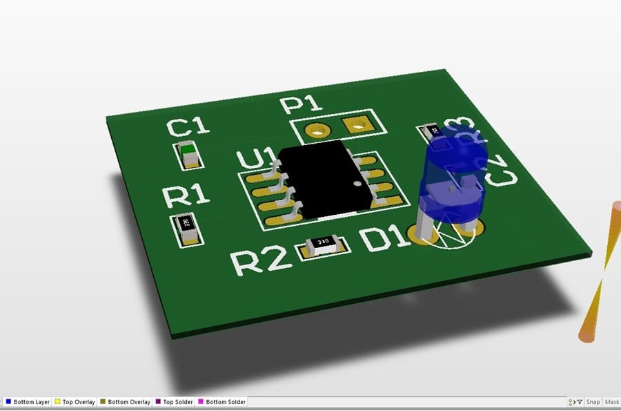
Once everything is placed, one can resize the board outline, re-define the board shape and take a look at what it looks like in 3D.
Hopefully, you have some STEP files or extruded 3D footprints associated with the PCB footprints. This really helps the visualization and the mechanical team, as you can export STEP files with fully loaded boards for fit checks against panels and such.
Routing this board goes quickly but for more advanced designs, Altium has a TON of useful features. Like in the schematic editor, it has a toggling mode and hotkeys that keep everything at your fingertips, maximizing efficient design.
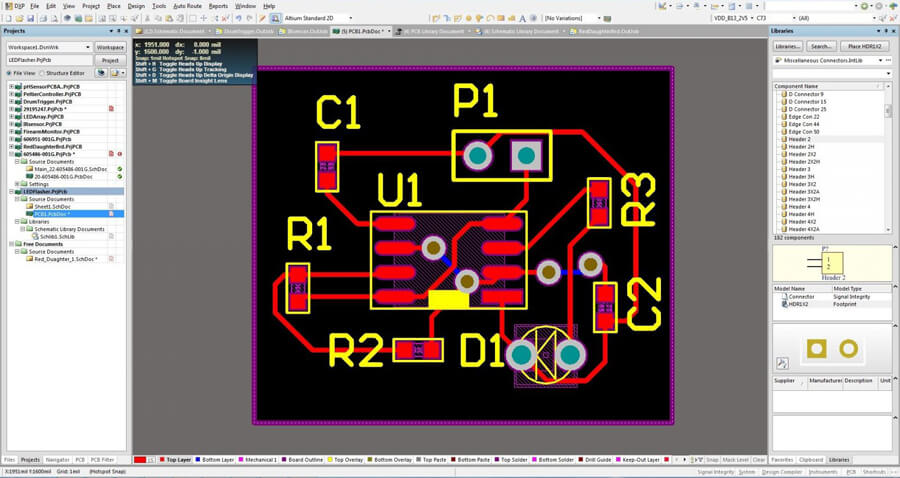
The design rule check is pretty standard and brings you back to the constraints. As long as everything is set correctly and you followed your own rules, it shouldn’t come back with any issues. But when it does find something, it’s pretty self-explanatory and double clicking on the item will take you straight to where the problem is on your PCB. Very useful!
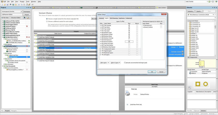
Generating the manufacturing files is done by creating one last thing called an output job file. You can add a bunch of files to be generated but the standard is drill and assembly drawings and the GERBERs. If you want to use a standard template for the drawing or create your own, you can do that on one of the mechanical layers. We have our own but it’s easy enough to use a standard one.
After that, edit each of the items and make sure they contain the right layers, then generate the file with folder structure and you’re done. Everything spits out into your project folder ready to be submitted to the manufacturer.
The Verdict
In the end, Altium Designer came out on top of the other programs and is our favorite PCB layout tool of the six programs compared.
As previously stated, Altium does all the little things right, despite being marginally less powerful than some of the other programs in certain areas. For example, the pad labeling is much more convenient in Altium than in other programs.
It is, however, quickly becoming the industry standard for professionals and the features that are lacking will surely improve as their customer-base and widespread feedback grow accordingly.

PCB School
Standards like MIL-PRF-55110, MIL-PRF-50884, and MIL-PRF-31032 exist to enforce reliability, traceability, and performance in environments where failure isn't acceptable.

PCB School
Flying probe testing has been the golden standard of functional testing for low volume, prototype runs since the late 80s and 90s. It effectively flips the approach of the traditional in-circuit (ICT) bed-of-nails fixture test, where a custom-built frame with hundreds of spring-loaded pins contact test points simultaneously.
PCB School
Double-sided Ball Grid Array (BGA) assembly maximizes component density without increasing board size, enabling high-performance designs for applications ranging from smartphones and IoT devices to medical and industrial electronics.
PCB School
Managing strain during press-fit connector insertion is essential for high-density PCB reliability. Discover best practices and how San Francisco Circuits ensures reliable assembly for HDI, mil-spec, and medical applications.

PCB School
San Francisco Circuits covers the 8 types of PCB vias including blind, buried, microvias, through-hole, stacked, & thermal vias - what they are, how they work, & where they’re used in advanced PCB design.

PCB School
Discover why NIST 800-171 compliance is essential for PCB manufacturers. As a PCB buyer, learn how this cybersecurity framework safeguards your sensitive data & ensure you are engaged with a boardhouse that meets these requirements.
