In the world of engineering and PCB design, “loss” is typically a downside (at least if it isn’t done intentionally as with thermal management and the usage of heat sinks). Whether it’s voltage, RF energy, optical signals, or any kind of amplitude from a given signal, loss will always occur in one form or another. Though we can’t avoid loss, we can certainly understand it and do our best to reduce it as much as possible. This article explores insertion loss: its properties, how loss occurs throughout a signal path in a system, and things we can do to minimize it.
The term “insertion loss” typically refers to the loss of signal strength as it passes through system-level cabling/components and PCB-level traces within high-speed (3GHz+) systems/optical fibers and PCB stack-ups. Sometimes referred to as “attenuation”, insertion loss is a measurement of the attenuation of a signal as it propagates down either an optical link or a transmission line. This number is typically expressed in terms of decibels (dB).
To maximize the energy transmission from point A to point B and minimize these transmission losses (including connectors and cabling), we must understand the core contributors of insertion loss. These contributors include:
Overall transmission length – For any kind of sensitive signals, especially high-speed signals, loss will scale proportionally with longer transmission lengths. This is primarily because of the added inline resistance. Additionally, it becomes harder to properly terminate each end with longer cabling, resulting in reflections due to impedance mismatches. And don’t forget that the longer the cable, the more prone it becomes to interference and inductive coupling as well. Thus, it’s always best to keep your lengths as short as possible.
Here’s an equation showing the relationship between dB loss and line length.

Related: read more about RF PCBs
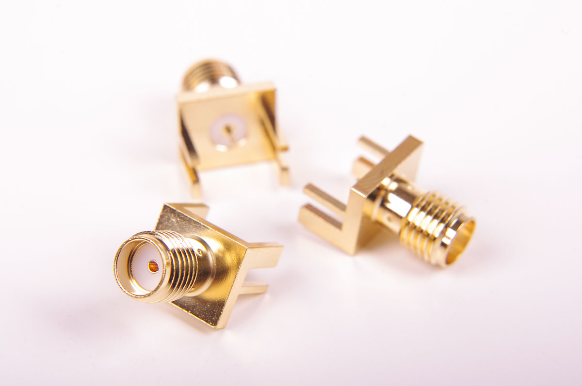
Connectors and cables – As previously stated, a system with longer line lengths will become harder to accurately terminate to minimize signal reflections, phase distortion, and return loss (the loss of signal power due to reflections). And when a system contains connectors for high-speed connections (like BNC) or coaxial cabling (shown below), these can also impact the overall loss of an RF or high speed signal path due to the same characteristics. Connectors and terminations can significantly reduce a systems Voltage Standing Wave Ratio (VSWR), or the ratio of the input impedance to the average characteristic impedance, represented by the signal loss due to reflections and phase distortion. This is mainly due to the surface mount or through-hole pads combined with the connectors pins which act as inductive and capacitive impedance discontinuities. Some connectors have better or worse VSWRs than others, but all are contributors to a system’s total insertion loss.
High-loss materials – Materials like dielectrics and conductors with plating can significantly increase a system’s insertion loss, as they dissipate extra power during transmission.
This can be apparent in connectors, cabling, and PCB traces or layers. Copper losses will stem from conducting surfaces, while dielectric losses are caused by a PCB’s internal prepreg and core layers. It’s often important to look at the ratio of these two losses and will vary based on PCB construction and frequency. Designing a proper PCB stack-up can drastically reduce the amount of loss including lamination thickness, copper selection/width, and the fiberglass weave composition. And depending on the signal frequency, a trace (acting as a conductor) on a PCB has a resistivity of approximately 0.72 x 10⁻⁶ ohms/inch. For a 5mil wide trace, this equates to roughly 0.1 ohm/inch for a standard 1oz copper pour. This added resistance will certainly introduce loss into the system, but it gets much worse at higher frequencies and with thinner substrates. A PCB with a 20mil thick substrate, for example, may have half the amount of loss as a PCB with 10mil thick substrate at higher frequencies (10GHz+). Even the type of copper selected can help reduce the insertion loss, especially when operating with thinner substrates.
Use our PCB stackup calculator / design tool to help design and visualize your multilayer PCB stackup from 4 to 14 layers.
Below are some plots taken by Rogers Corporation (Advanced Circuit Materials Division), showing some of these comparisons. The plot on the right demonstrates an insertion loss comparison of 20mil microstrip transmission line circuits using standard RO4350B laminate and comparing performance of bare copper to ENIG PCB surface finish.
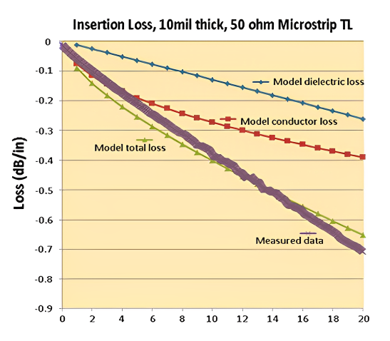
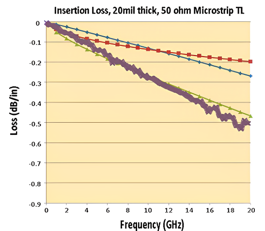
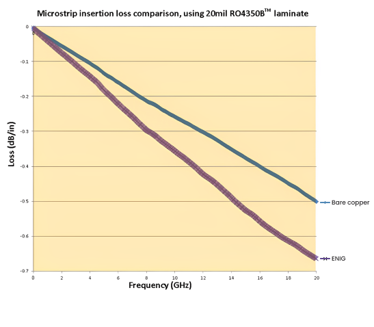
Image Source: Rogers Corporation, John Coonrod
Higher frequency systems – As shown in the plots above, frequency has a major impact on the amount of insertion loss in a system. Though transmission length, poor terminations and added interconnects like connectors/cabling, and high-loss materials all contribute to a systems insertion loss, the amount of loss scales up with frequency. For signals in the 3GHz to 5GHz domain, mismatched impedances will have the largest impact on insertion loss. But for systems operating at 10GHz or more, the materials used in a PCB stack-up will tend to have a larger contribution to insertion loss, especially if there are vias containing parasitic inductance/capacitance. Additionally, the “skin effect” comes into play at higher frequencies as well. This effect is essentially a copper trace or plane concentrating its transmission more towards the “surface” of the copper, making for a less effective use of the cross-functional area, adding additional resistance. Below is a table that provides the relative “skin depth” at various frequencies.
|
ƒ |
1 MHz |
4 MHz |
15 MHz |
50 MHz |
100 MHz |
1 GHz |
10 GHz |
|
δ |
2.6 mils |
1.3 mil |
0.7 mil |
0.37 mil |
0.26 mil |
0.08 mil |
0.026 mil |
Related: read more about electronic interconnect design considerations
As we’ve seen, there are many instances in which insertion loss can occur throughout a system’s signal path. However, there are ways to combat this. Understanding the trade-offs and design practices can allow a designer to greatly lower a systems insertion loss while striking a good balance with regards to production costs and signal integrity. Let’s quickly cover these considerations.
Lastly, many of these considerations can involve trade-offs in terms of production costs (including PCB fabrication/assembly and the quality of system-level and board-level components). Consulting with an experienced PCB fab/assembly provider like San Francisco Circuits can help balance these trade-offs and maximize the performance of your application.
