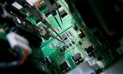
Recent developments into miniaturizations have been a major cause of the great momentum in the electronic industry’s expansion. As miniaturization continues to propel the industry, fabricating electronics and manufacturing PCBs is becoming highly challenging. The most challenging aspect of PCB fabrication is the incorporation of high-density vias and through holes used as interconnects. The through holes are used to mount the electronic components, which make up the circuits.
As the packing density of the through holes in the PCB assembly line increases the demand for smaller holes increases respectively. Two main technologies that are used to produce accurate and repeatable holes of microns in diameter are mechanical drilling and laser drilling. The through hole diameters can range from 50-300 microns and run about 1-3 mm deep using these PCB drilling techniques.
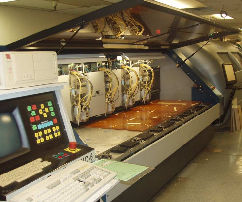
PCB Drill Room
The drill press consists of a high-speed spindle, which rotates at speeds of about 300k RPM. These speeds are essential to produce the required accuracy for micron-level drilling on the PCB.
To maintain accuracy at high speeds, the spindle makes use of an air bearing and a direct drill bit assembly, which is held by a precision collet chuck. Additionally, the vibration of the tip of the bit is controlled within a 10-micron range. In order to maintain the exact position of the hole on the PCB, the drill is mounted on a servo table, which controls the motion of the table on the X and Y-axes. A tunnel actuator is used to control the motion of the PCB in the Z-axis.
As the pitch of the holes in the PCB assembly line is constantly decreasing and the demand for higher throughput is respectively increasing, the electronics to control the servo may lag behind at some point in time. The use of laser drilling to create through holes for manufacturing PCBs helps reduce or eliminate this lag and is the next generation’s requirement.
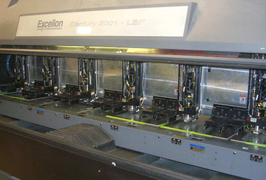
PCB Drill Room
Laser drills used in the PCB fabrication process consist of a complex set of optics, which are used to control the pinpoint accuracy of the laser, required to make a fine hole.
The size (diameter) of the hole to be drilled in the PCB is controlled using the aperture of the setup and the depth of the hole is controlled by the time of exposure. Also, the beam is split into various energy bands to further provide control and precision. A moving focal lens is used to concentrate the energy of the laser beam exactly at the drilling location. A Galveno-sensor is used to accurately move and position the PCB with high speed and accuracy. Galveno sensors capable of switching at speeds of 2400 KHz are currently used in the industry.
Additionally, a novel method known as the direct exposure technique can also be used to drill holes in the circuit board. This technique is based on the concepts of image processing, where the system increases the accuracy and speed by creating an image of the PCB and converting that image into a position map. The position map is then used to align the PCB under the laser for the drilling process.
Advanced research in image processing algorithms and precise optics will further improve the throughput and yield of PCB fabrication and high speed drilling used in the process.
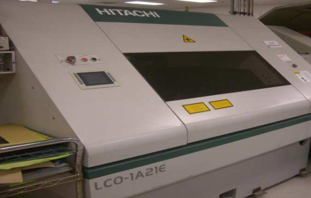
PCB Laser Drilling
Or EMAIL US to discuss & quote your project
PCB School
Standards like MIL-PRF-55110, MIL-PRF-50884, and MIL-PRF-31032 exist to enforce reliability, traceability, and performance in environments where failure isn't acceptable.
PCB School
Flying probe testing has been the golden standard of functional testing for low volume, prototype runs since the late 80s and 90s. It effectively flips the approach of the traditional in-circuit (ICT) bed-of-nails fixture test, where a custom-built frame with hundreds of spring-loaded pins contact test points simultaneously.
PCB School
Double-sided Ball Grid Array (BGA) assembly maximizes component density without increasing board size, enabling high-performance designs for applications ranging from smartphones and IoT devices to medical and industrial electronics.
PCB School
Managing strain during press-fit connector insertion is essential for high-density PCB reliability. Discover best practices and how San Francisco Circuits ensures reliable assembly for HDI, mil-spec, and medical applications.

PCB School
San Francisco Circuits covers the 8 types of PCB vias including blind, buried, microvias, through-hole, stacked, & thermal vias - what they are, how they work, & where they’re used in advanced PCB design.

PCB School
Discover why NIST 800-171 compliance is essential for PCB manufacturers. As a PCB buyer, learn how this cybersecurity framework safeguards your sensitive data & ensure you are engaged with a boardhouse that meets these requirements.
