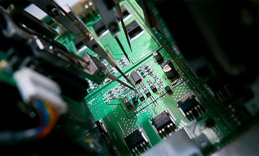
PCB designs containing a low-power blinking LED for something like status indication, are pretty commonplace in today’s world, but what if that LED required over 10 amps of current? Or how about 20 amps? Or what if the voltage needed to drive it was over 100V? At what point is a load considered high voltage or high current, and what does that mean for the PCB design process? There are several factors that must be considered when specifying components and laying out a PCB for these kinds of conditions, so let’s jump right in.
Current is carried through copper traces and planes, and that’s pretty common knowledge. However, those traces and planes have a resistance associated with them and, depending on the amount of current, could negatively impact the performance of a board and in some cases, even damage the board and components. In extreme conditions, even the machine and its operator can be at risk if a board fails.
The longer and narrower the PCB trace, the higher the trace’s resistance–resulting in a larger voltage drop across the two signal’s endpoints. A trace or plane will also increase in heat when carrying larger amounts of current, which can impact nearby sensitive components while also putting the integrity of the copper at risk.
A related article “The Importance of PCB Trace Widths in PCB Design” provides a high-level view of trace width, length, and styles used in a variety of applications. One of the sections describes how a PCB trace width can be calculated and used to optimize voltage drop. The same calculations apply here. If the designer can plan accordingly and use the application’s current requirements to drive the minimum trace widths for a given trace length, then the voltage drop can be quantified and laid out with confidence. It helps to know what PCB characteristics impact these values and how they can be changed in the design. When the trace’s current is beyond what is practical in terms of width or area, then other strategies can be used to maximize the copper.
Typical copper weights are set as a default to 1 ounce (or 1.4mil thickness), however this copper thickness can generally be increased on a given layer. Copper weights for outer layers can be as high as 15 ounces (or 21mils thick). This will not only drive the overall PCB thickness, weight, and fabrication cost but will also require more spacing between pads and components due to the etching process, so there’s a balance that must be considered when selecting a thicker copper weight.
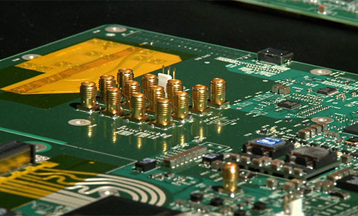
Another lever that can be pulled to increase copper volume for a given power signal, is spreading the trace or plane across multiple layers and tying them together with a technique called via stitching. Via stitching is common in communications devices where shielding and noise/crosstalk suppression is important, but it also helps with thermal management and reduces a trace’s overall resistance. This is fairly common for power components containing thermal pads on the case and helps to lower the temperature at the pad-to-pad junction.
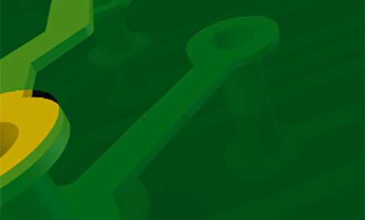
The same idea can be applied to a power plane or trace, which can be mirrored on multiple layers and tied together with several vias, as shown in Figure 1. And remember, vias themselves are like micro-resistors, so make sure the via’s diameter connecting the layers together isn’t too small, and make sure there are enough vias to help transfer the heat.
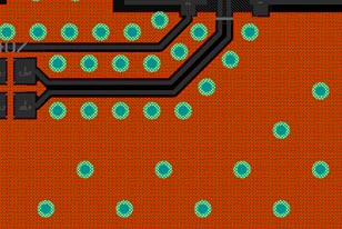
Figure 1. Example of Via Stitching for Thermal Management
While some PCB design tactics can be used to manage the thermal properties of a PCB, working with your PCB vendor and selecting an appropriate board layer stack-up can also greatly reduce board temperatures produced by large currents. Choosing stack-up materials that results in a lower Coefficient of Thermal Expansion (CTE) can limit the expansion and contraction of the PCB when heated or cooled, which will improve the durability of the PCB and help to minimize structural faults. For applications where current is high and temperature is difficult to manage, metal core PCBs filled with aluminum, copper, or other special allows can help to spread the heat throughout the entire PCB
Learn more about: Metal Core PCB(MCPCB)
Some PCB design software gives visualization on thermal distribution, such as Altium Designer. If you have the tools available, some of these features can be highly effective at providing a snapshot of potential hot spots and how to manage them. Figure 2 shows Altium’s PDN Analyzer tool visually demonstrates heat distribution throughout the PCB.
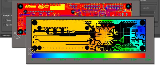
Figure 2. Altium Designer’s PDN Analyzer (courtesy of Altium.com)
In addition to maximizing copper area for a given signal, other non-PCB cooling techniques can be employed, such as heatsinks (passive cooling) or adding airflow (active cooling). Heatsinks are generally used in conjunction with components that require extra power dissipation, but can also be mounted to exposed copper traces or planes along with a thermal paste which allows for optimized thermal transfer. Airflow is usually ideal and while it can be complicated and more costly to implement, is usually worth the effort.
And finally, it’s always best practice to incorporate fail-safe circuits and redundancy in the event a high current application fails to protect the hardware and nearby operators. Soft-start circuits, overcurrent protection and fuses, current monitors and regulators, relays and interlocks, and general surge protection are examples of components that can be used to monitor, protect, and disconnect loads in the event of a fault. Functional tests with simulated loads performed at the PCB vendor can also help with preventing failures and unsafe conditions during normal use.
Designing for high voltage is quite a bit different than high current applications, and can be trickier. First off, high voltage in the AC realm is considered anything over 1000V but for DC voltage, it’s a lot lower. According to the Occupational Safety and Health Administration (OSHA), anything equal to or more than 50V is hazardous for both AC and DC applications. And let’s not forget that AC voltage consists of a Root Mean Square (RMS) parameter that, when calculating the peak value, it’s peak will be around 1.4 times higher. Many things must be considered when designing for higher voltage applications, such as clearances between exposed contacts and copper to prevent arcing, insulated wiring or cabling, and making sure that the right materials (substrates and laminates) are chosen in the board stack-up.
First, let’s look at the most important one: clearances.
It’s essential for high voltage PCB design, UL60950-1(USA), CSA22.3 (Canada), or any other applicable standard regarding high voltage design requirements, to be reviewed and understood. This includes information on minimum clearances and creepage distances between two circuits (or contacts). Since voltage is a potential difference, electronics will want to find a way to get from the higher potential to the lower potential, even if that means “jumping” across an air gap. This is generally referred to as arcing, a dangerous event that can damage boards and cause fires.
The best way to prevent arcing from occurring is to follow the creepage guidelines seen in Figure 3.
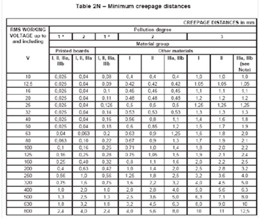
Figure 3. Table 2N – Minimum Creepage Distances from UL60950-1
Let’s quickly walk through this table. The pollution degree specifies the pollution and non-conductive contaminants that might exist in the application. Most applications involving PCBs will be a pollution degree of 2, which automatically has us looking at the “printed boards” column “I, II, IIIa”. As you can see, the minimum creepage stays at 0.04mm up until 50V, where it increases from there.
Clearance on a PCB is defined as the minimum direct distance through air between two conductors, while creepage is the length of distance between the conductors along the surface of the PCB. And, as seen in Figure 3, the minimum values of these distances are determined by the working voltages. The peak DC voltage will determine the clearance while the RMS value of AC voltage will determine the creepage distance.
It’s not always easy to meet these minimum clearance and creepage values but some strategies include placing components on both sides of a PCB to maximize distance between two copper surfaces, as well as using various thicknesses of insulating materials to maximize creepage distance.
Conformal coating, a common practice in high voltage circuits, is the application of a non-conductive, dielectric insulation to your PCB’s surface. In addition to helping with arc prevention and high voltages, it also adds several other benefits such as thermal, structural, and environmental protection. IPC-A-610 is the typical standard that is referenced for these coatings but more stringent standards can be applied, depending on the application.
And while configuring the board’s stack-up, depending on the power requirements, it may be useful to consider moving away from the very commonly used FR-4 substrate material. Polytetrafluoroethylene (PTFE) and Polyimide substrates are rated for higher temperatures and generally provide more support for higher voltage applications. And prepreg, the fiberglass which is pre-impregnated with resin that holds each layer together in the PCB stack-up, also comes in some higher rated materials and glass styles, such as 1080 or 2113. Work with your PCB vendor to see what options are available for higher voltage and power materials.
And one of the best insurance policies you can provide during the manufacturing process is a test to ensure that the PCB has good isolation and spacing between high potential surfaces. This test is typically referred to as a hipot, or dielectric, test. It’s the opposite of a continuity test and checks to see that, at increased voltage levels, no current flows from any two, unconnected conductors. Performing this test during the production process will help weed out those boards containing defects and help to minimize field failures (and unsafe conditions) while increasing the PCB’s overall reliability.
The best way to manage copper pads, copper traces, and copper planes in high-load applications is to test for, and monitor, the following:
If you take into account the following areas above, you'll be well on your way to test and ensure your new PCB has everything it needs to function well with high-load applications.
Looking for help with your next PCB project? San Francisco Circuits specializes in many PCB technologies from production to prototype quality. And when it comes to PCB traces, we can make sure you get what you need to have the best device performance.
PCB School
Standards like MIL-PRF-55110, MIL-PRF-50884, and MIL-PRF-31032 exist to enforce reliability, traceability, and performance in environments where failure isn't acceptable.
PCB School
Flying probe testing has been the golden standard of functional testing for low volume, prototype runs since the late 80s and 90s. It effectively flips the approach of the traditional in-circuit (ICT) bed-of-nails fixture test, where a custom-built frame with hundreds of spring-loaded pins contact test points simultaneously.
PCB School
Double-sided Ball Grid Array (BGA) assembly maximizes component density without increasing board size, enabling high-performance designs for applications ranging from smartphones and IoT devices to medical and industrial electronics.
PCB School
Managing strain during press-fit connector insertion is essential for high-density PCB reliability. Discover best practices and how San Francisco Circuits ensures reliable assembly for HDI, mil-spec, and medical applications.
PCB School
San Francisco Circuits covers the 8 types of PCB vias including blind, buried, microvias, through-hole, stacked, & thermal vias - what they are, how they work, & where they’re used in advanced PCB design.

PCB School
Discover why NIST 800-171 compliance is essential for PCB manufacturers. As a PCB buyer, learn how this cybersecurity framework safeguards your sensitive data & ensure you are engaged with a boardhouse that meets these requirements.
