There are a number of factors to consider with the mechanical aspects of a PCB. In this article, we are going to dive into the various ways a PCB designer can help to deliver a board meeting mechanical and thermal requirements while staying competitive on cost.
Unnecessarily tight constraints on the board will be a cost driver. Meanwhile, an insufficient set of physical parameters leaves the potential for a board that does not meet the necessary requirements in the field.
One's goal is to find the sweet spot between precision and price. Believe it or not, that is possible to do.
The board outline must fit within its enclosure. The product communicates with the outside world through connectors mounted on the board that poke outside of the housing. And, connector slots on the PCB should have specific dimensions for the depth and width requirements.
Remember to consider any internal radii and allow for an over-cut as a relief so that the connector doesn’t bottom out on the radii before fully engaging the pins on the land pattern.
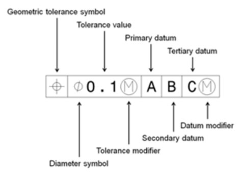
Geometric Dimensioning and Tolerancing frame showing a positional tolerance.
The mounting holes should be dimensioned as a bolt pattern using positional tolerance as shown in the figure above. The primary datum for the bolt pattern should be one of the holes and the other holes be directly dimensioned from that other hole. It’s wise to have this be coordinated with the drawing of the enclosure to ensure proper alignment. The ideal outcome is to prevent an accumulation of tolerances where PCB meets the design requirements but is not overly constrained.
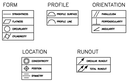
The typical GD&T symbols found on a mechanical outline drawing.
Non-plated holes for tooling or other purposes can have a tighter diametral tolerance than plated through holes. The non-plated holes are drilled as a separate operation after all of the plated holes and lamination cycles. Extra clearance around those non-plated holes increases the yield through fabrication.
Incorporating geometric dimensioning and tolerancing tells the story of what is important and where deviations from the nominal can be accepted. Every board that meets the mechanical design specification should fit together with the enclosure. Using GD&T is a great way to tailor those specifications from the top down while keeping the yields at an acceptable level. The American Society of Mechanical Engineers (ASME) conducts official training on this but there are many other short courses available online.
Working from the middle layers outward, design the stack-up so that there is a mirror image as you work your way towards the outer layers. It is not always possible to use the same thickness of dielectric and metal layers. It’s important to use thicker copper for power and ground planes. Thicker copper doesn’t readily support etching of fine lines, so our trace layers end up using a thinner sheet of copper. In practical terms, we’re actually designing the space between the copper because that is what is being removed during the fabrication process.
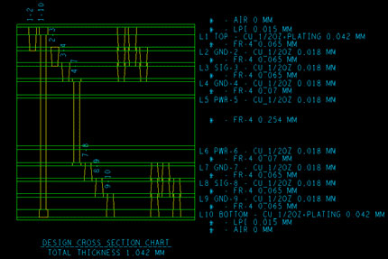
A typical 10-Layer HDI stack-up used for consumer electronics
It's also important to note, the outer layers will have to be plated up in order to plate copper into the barrels of the vias. In most cases, a fabrication shop has to create a core via for sequential lamination, the outer layers that make up the span of the core via may have to be treated as if they were outer layers for the same reason. Stacking the micro-vias may invoke a minimum copper weight. When you’re doing these complex high density interconnect (HDI) constructions, don’t go it alone. Make sure your vendor can actually build the board based on the stack-up, line-width, and air-gap goals.
One of the common challenges with PCB stackups is the overall PCB thickness tolerance.
As the products themselves shrink in size, the z-stack of the various parts including the board become more important. One of the features of high-speed, high-frequency, materials is better thermal stability over temperature. From a physical design standpoint, it would be nice if the thickness could be constrained to the same degree as a sheet of aluminum. Given the number of different materials going into the press, this is not possible. The thickness can be held to +/-10% of the nominal value under most circumstances.
For more information view our PCB Stack-Up Guide and use our PCB Stack-Up Calculator / Design Tool to help when planning your own.
PCB flatness is a critical requirement, especially for boards using surface mount devices. Ball grid arrays are particularly sensitive to PCB flatness as the pin-count rises. Once a board has turned itself into a “potato chip”, it can be flattened under heat and pressure, but the underlying reason why it was in the twisted state remains. It will tend to return to the non-flat condition when it goes through the soldering process.
Two methods can be employed to ensure even metal distribution, copper flood and copper thieving.
Pouring the ground plane on all of the layers is the first that comes to mind. The ground plane can work against you if the copper is isolated or if it forms sections where it cannot be staked to other ground layers. A sliver of copper between two traces will increase coupling between those two traces if it is not supported with vias along its length.
When using through-hole technology, the vias interrupt every layer and that will not be ideal for the voltage plane(s) to have so many voids. There may be a routing layer that is too dense for sufficient via penetration. When that is the case, the copper can still be equalized on a layer-by-layer basis by using copper thieving.
There is something pleasing about using the golden ratio for the shape of the copper thieving. Offsetting the rows prevents seams while rounding off the corners makes the etch process more organic.
Remember that the break-off edges of an assembly panel will also contribute to the flatness or warpage of the board so this is often a location for metal thieving even if the actual PCB is fully flooded on all of the layers. The image above shows a wider pull-back from the large radius due to a route keep-out. Note the outline at the top left, the “Mickey Mouse ears” allow the mating connector to sit flush in the slot.
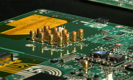
Back panels are not the only type of boards that can make use of a good stiffener or two. Any board that is under a millimeter in thickness is likely to be a bit flimsy. Aluminum crossbars or a complete perimeter frame can bolster a board while acting as a thermal path. Incorporating the stiffener with the mounting hardware enhances both of those benefits.
“Additional gussets may be added at stress points caused by heavier components …”
The contact area for the stiffener should be plated copper that is part of the chassis ground. Soldermask and silkscreen should not occupy this area in order to present a flat metal mating surface. Additional gussets may be added at stress points caused by heavier components such as heat pipes and sockets.
Shielding cans for electro-magnetic interference (EMI) can also stiffen an area of the PCB. Ball Grid Array (BGA) packages used in harsh environments will benefit from the use of underfill. Aside from glueing the package down, the underfill has the effect of easing the thermal stress when the device package has a different coefficient of thermal expansion (CTE) than the PCB material. This is particularly important when using chip-on-board (COB) technology. The underfill keeps the localized area more stable over temperature swings. This reduces strain on the solder joints. The finer pitch devices are most susceptible to this type of failure as the ball diameter shrinks along with the pitch.
Metal core PCBs have a stiffener built right into the stack-up. And boards that dissipate a lot of heat will benefit from this technology–linear power supplies and LED lighting boards for example. The metal can be sandwiched between dielectrics or used as a baseplate. Aluminum is the most common base material. Copper uses less volume for the same performance but is a higher-cost raw material and is more difficult to machine.
Read more about heavy copper PCBs.
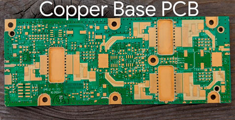
A four-layer PCB with three layers of one-ounce copper with GETEK dielectrics and one of solid 45-oz Cu base.
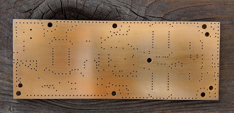
Bottom Side of the high-power RF amplifier
These metal layers go well beyond the two or three ounce copper found in many high performance PCBs. The metal is not etched into a circuit pattern. The whole layer is a solid ground plane. The signal vias are generally micro-vias that do not penetrate the metal core or base. Using metal in this way stabilizes a PCB against bow and twist while maintaining greater dimensional accuracy of the z-stack.
In summary, using concise dimensions provides the PCB fabricator with the design knowledge to execute compliant boards. A balanced stack-up will help keep the board flat while stiffeners will lock the board into a planar flatness that enhances surface mount component assembly and acts as a heat spreader. Finally, incorporating a slab of metal in the center or on the bottom of the PCB will achieve all of those aims.
PCB School
Standards like MIL-PRF-55110, MIL-PRF-50884, and MIL-PRF-31032 exist to enforce reliability, traceability, and performance in environments where failure isn't acceptable.
PCB School
Flying probe testing has been the golden standard of functional testing for low volume, prototype runs since the late 80s and 90s. It effectively flips the approach of the traditional in-circuit (ICT) bed-of-nails fixture test, where a custom-built frame with hundreds of spring-loaded pins contact test points simultaneously.
PCB School
Double-sided Ball Grid Array (BGA) assembly maximizes component density without increasing board size, enabling high-performance designs for applications ranging from smartphones and IoT devices to medical and industrial electronics.
PCB School
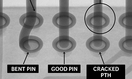
Managing strain during press-fit connector insertion is essential for high-density PCB reliability. Discover best practices and how San Francisco Circuits ensures reliable assembly for HDI, mil-spec, and medical applications.

PCB School
San Francisco Circuits covers the 8 types of PCB vias including blind, buried, microvias, through-hole, stacked, & thermal vias - what they are, how they work, & where they’re used in advanced PCB design.

PCB School
Discover why NIST 800-171 compliance is essential for PCB manufacturers. As a PCB buyer, learn how this cybersecurity framework safeguards your sensitive data & ensure you are engaged with a boardhouse that meets these requirements.
