As new electronic devices are developed and more features need to be added, the space on a PCB becomes even more important. And as devices need to be smaller and smaller due to consumer demand, PCBs have to be dense to fit all the components. Which is why proper use of microelectronics best-practices in PCB production (design/layout, fabrication & PCB assembly) ensures devices function well even with reduced form factors.
PCB design is at the nexus between electrical and mechanical design, making specific build requirements unique. A PCB design expert may tell you to start out with simple two and four-layer PCBs with plated through-hole (PTH) components. Then, they would tell you to progress to surface mount technology (SMT) and eventually to high density interconnect (HDI) designs. And maybe you would start with analog or digital designs and work towards mixed signal efforts.
That may have been the usual path a designer would take in the past, but that ship has long since sailed. Today’s beginner to intermediate PCB designer needs all of those tools mentioned above and then some. If you look at consumer demands and industry requirements, no one is asking for 1990’s technology. If you want to be the PCB designer of “tomorrow,” then the learning never ends.
The new world of microelectronics has ubiquitous high speeds and high frequency technologies located in every corner. Transistors come by the billions and now fit on a business card. PCB layer counts are well into the double digits. Linewidths are becoming so small they seem to vanish. Microns are being used because thousandths of an inch is too large to measure. Yes, microelectronics are changing, so let’s start with the basic building blocks you need to know.
The components for “simple” boards of the past would be difficult to source. Even if you could find them, they would lead to bulky and power-hungry designs. And when it comes to surface-mounted devices, the pin pitch gets tighter with every new generation. The common components have pins around the perimeter with typical center-to-center dimensions of 0.5 and 0.4 millimeters.
Read More: PCB COMPONENT OVERAGES & SOURCING CHEAT SHEET
PTH devices were commonly made with pins centered on 2.54 mm. The Dual In-line Packages (DIP) had widely spaced pins on only two sides. Something between eight and twenty pins were common; fourteen pins are the most typical of the DIP packages. Design work was much easier then, but what about now?
Today, the modern quad flat-pack (QFP) parts have little surface mount “gull-wing” leads all the way around. The central area within the perimeter normally has a large pin that is tied to the ground net for an additional thermal path. The pin count starts at 16 (plus one) and easily gets to 128 pins. To make it more compact, chip vendors tuck the leads under the device. This is known as a quad flat no-lead, or QFN for short.
We’ve covered devices with pins all around and in the middle, but the density train doesn’t end with that technology. The entire bottom of modern chips are connected to the PCB with a grid of pins that have no leads at all. Instead, spheres of solder are attached to the bottom of the device in a grid pattern–these are called ball grid array (BGA) packages. Ball grid array packages have quickly become the most popular packaging choices used in microelectronics.
The earliest BGA packages came with ball-to-ball pitches of 1.27 millimeters; half the spacing of traditional components. A typical via could be used to fan-out and route these packages. To decrease the size of the BGA, the pins were crowded together down to one millimeter pitch. Next came 0.8 mm and then 0.65 mm, which is the finest pitch that can be supported with normal PTH technology boards.
.jpg)
Figure 1. PCIE card with an 802.11n 3x2 MIMO radio circa 2010. The baseband chip is not populated to reveal a 360-pin footprint as an example of the finest pitch BGA device that can be supported with through-hole technology.
Since high-reliability PCBs (categorized as Class 3 by the IPC) require a larger capture pad for the vias, the party ends with 0.8 mm pitch BGA packages for those applications. For a long time, BGA packages were not considered reliable enough for such applications. They have since found their way into the automotive industry, but mainly to the extent they support through-hole vias. As silicon areas shrink, from 0.5 mm, 0.4 mm down to 0.35 mm, the edge rates of circuits go up and the signal integrity challenges escalate.
When observing a PCB, you might notice traces running between the pads of the BGA. As the ball-pitch decreases, those channels are lost. The area for the fan-out via is also lost. The fine pitch BGA footprints use microvias inside the SMD pads. The further into the middle of the BGA package you go, the deeper into the board you have to go to find a more suitable routing channel. And as a result, stacking is used for the microvias.
Stacking up those microvias is definitely a cost-driver.
Read More: ELECTRONIC INTERCONNECT DESIGN CONSIDERATIONS
Connectors have some staying power in through-hole technology because of the stress they endure as they are engaged and disengaged. Even so, there is a trend towards using alignment pins along with hybrid solutions that mix through-hole and surface mount pads in the same connector. A great example of this architecture is USB type-C.
When you encounter components like the USB-C connector, there are often some very specific dimensions on the data sheet. Non-plated holes may have very tight tolerances, which can be captured in the pad-stack. There also may be a slot in the board for a mid-mount connector with a unilateral tolerance.
Soldermask, paste stencil apertures, and local fiducial marks are critical to PCB assembly.
This information is important to capture and preserve so it goes into the process of creating the fabrication drawing. A vendor needs to know where to be precise with milling and drilling operations. As a result, some connectors require hard gold or a generous area to engage the mating connector. And the data can be lost if it is not actively managed in the footprints
Small logic circuits, and Axial leaded resistors and capacitors will probably remain popular because they serve an ecosystem for the hobbyist and the low-tech development types of printed circuit boards. Meanwhile, the processors and other advanced chips have left this space behind.
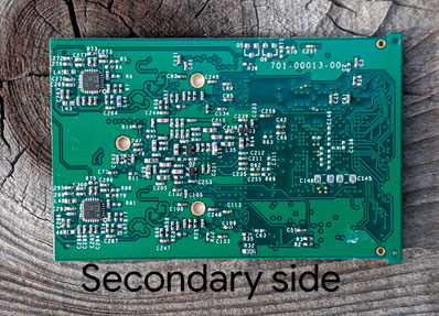
Figure 2 shows the same PCB as Figure 1, but from the bottom side. All components are surface mount with decoupling capacitors for the BGA package placed on the secondary side, along with several delay lines and small ICs. This configuration is common in double-sided BGA assembly to maximize component density while preserving signal integrity and power distribution performance.
This space has been left behind for more advanced chips due to the size of the vias used for the old-school boards not supporting requirements of the latest generation of devices. One-by-one, the plated through hole components of yesteryear are becoming obsolete. Anyone wishing to make a career out of PCB design is going to have to catch up and keep up with the latest technologies available in microelectronics.
Junior PCB designers are going to have to be versed in micro-vias due to the advancements in microelectronics. Implementing micro-vias in a design comes with a few dependencies. The first concern is that the small diameter of the microvia is difficult to plate unless the hole is shallow. Even a one-to-one ratio of depth to diameter is a challenge.
The typical PCB factory can manage a 100 micron diameter hole size if the thickness of the dielectric is 65 microns or less.
So, the layers have to be quite thin. When a thin layer is used, the geometry of a controlled impedance transmission line also decreases. In order to achieve the thin linewidth, the fabricator has to start with a thinner copper foil. For a top-layer trace, it makes more sense to move the reference plane from layer-2 down to layer-3 and create a void on layer-2 below the run of the transmission line.
Rather than making a void in the layer-2 copper, it is advisable to use a route-keep-out shape so the area remains free of inadvertent routing or copper flood if the shape has to be replaced. This will happen globally when the board outline is revised. Failsafe practices include the use of keep-outs for components and routing as necessary. Design intent will survive future editing even if it is someone else doing the project. That will include capturing design constraints that cover minimum line width and air-gap as well as any length requirements.
The beauty of a microvia is that they lend themselves to being placed within the SMD pad, which allows for a tighter placement since there’s no requirement to account for the fan-out via. While it is possible to fill and cap a traditional mechanical via, their larger size makes them best suited to the center pad of the QFP and QFN packages. Simply put, microelectronics require micro-vias.
A typical implementation of micro-vias would be an eight-layer board.
The first step is to create a four-layer board that will eventually become layers 3, 4, 5 and 6 of the finished board. Then the next step is to build up another layer pair by sandwiching the 4-layer “core” with a layer of prepreg above and below. That step involves a second lamination cycle. Then a laser system is used to create the micro-vias which are plated and the process repeats.
Starting with four layers, going up to six, and finishing with eight layers uses a total of three lamination cycles. The end product has micro-vias from layers one to two and another spanning from two to three. Then there is the core which uses a standard mechanical drill size followed by two more build-up layers from six to seven and then seven to the bottom.
Lamination cycles involve a very expensive piece of equipment known as a press. The press is not a quick process; certainly not as quick as the drilling or plating steps. This makes sequential lamination a costly endeavor with a longer lead time. It is highly advisable to work closely with your pcb fabrication vendor as you use HDI technology.
Working with the right partner makes all the difference in your final microelectronics project.
Have questions about microelectronics?
Drop us a line–we’d like to learn more about your next project. San Francisco Circuits specializes in advanced technologies like metal core PCB and flex PCB using advanced PCB surface finishes in both production and prototype quantities.
PCB School
Standards like MIL-PRF-55110, MIL-PRF-50884, and MIL-PRF-31032 exist to enforce reliability, traceability, and performance in environments where failure isn't acceptable.
PCB School
Flying probe testing has been the golden standard of functional testing for low volume, prototype runs since the late 80s and 90s. It effectively flips the approach of the traditional in-circuit (ICT) bed-of-nails fixture test, where a custom-built frame with hundreds of spring-loaded pins contact test points simultaneously.
PCB School
Double-sided Ball Grid Array (BGA) assembly maximizes component density without increasing board size, enabling high-performance designs for applications ranging from smartphones and IoT devices to medical and industrial electronics.
PCB School
Managing strain during press-fit connector insertion is essential for high-density PCB reliability. Discover best practices and how San Francisco Circuits ensures reliable assembly for HDI, mil-spec, and medical applications.

PCB School
San Francisco Circuits covers the 8 types of PCB vias including blind, buried, microvias, through-hole, stacked, & thermal vias - what they are, how they work, & where they’re used in advanced PCB design.

PCB School
Discover why NIST 800-171 compliance is essential for PCB manufacturers. As a PCB buyer, learn how this cybersecurity framework safeguards your sensitive data & ensure you are engaged with a boardhouse that meets these requirements.
