Designing a printed circuit board (PCB) that efficiently and effectively achieves target specifications is a challenge that requires close attention to a great number of details.
The challenge escalates exponentially when you are designing a product that utilizes multiple boards that need to connect to each other through electronic interconnects. While you may feel like tearing out your hair as you try to accommodate all the variables in a multi-board assembly, there are some tried and true tips and considerations that can make the process smoother and less nerve-wracking.
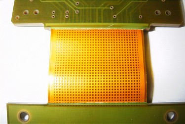
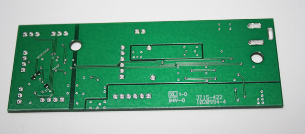
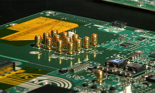
Multiple PCBs
Connected via Rigid-Flex PCB Interconnect
While true that a multi-board solution may not be the optimal approach in terms of functionality, there are reasons why you have to use this approach.
It could be something as simple as accommodating for a strict form factor or the need to easily isolate power or sensitive signals. You may be charged with using an “off-the-shelf” board to talk to specific components or a custom board (such as LCD displays). Other reasons for stacking boards could include designing for future expansion (like the common Arduino shields), having multiple design configurations (maybe a basic version and an advanced version) or just making your design modular in general (a sort of mix-and-match).
A separate board may be deployed to address a particular task in a trace-specific application, such as trace routing for capacitive touch, inductive charging, or custom resistances.
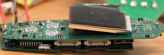
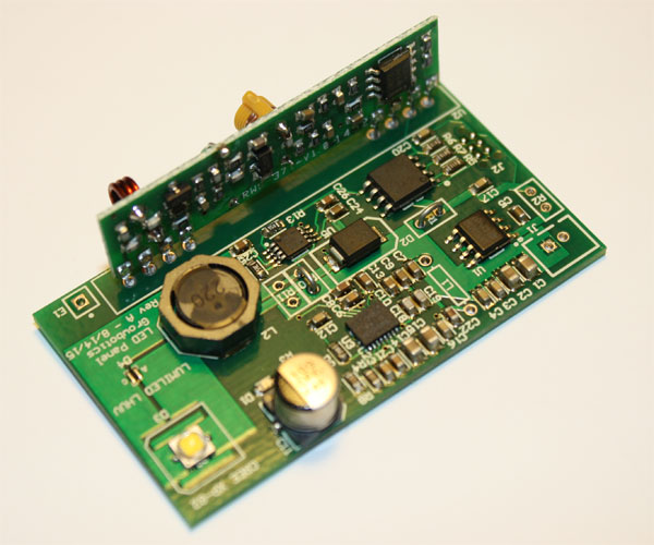
Stacked PCBs
Whatever the reason, keeping in mind some best practices and focusing on details will help you achieve your product goals with minimal difficulty.
For example, when multiple boards need to talk to each other, the pin count will increase and component density, which can cause signal integrity issues, adds to testing time, creating a more complex product to manufacture. Life-cycle durability of the finished product can also be affected by an increase in boards connected to one another.
There will be some bumps in the road, but if you stick to a good plan and employ sound principals to reduce common pitfalls and risks, the final printed circuit board, PCB interconnect(s) and application will reflect that same level of quality preparation.
Partnering with an experienced PCB manufacturing and assembly provider with engineers that have worked with and modified multiple layouts in preparation for fabrication and assembly of electronic interconnects is crucial for complex projects.
Successfully taking your elaborate PCB designs from layout to PCB assembly is the core value that comes from partnering with San Francisco Circuits for your next project - from flex PCB to bare boards, we are your one-stop shop for intricate, advanced printed circuit technologies.
Putting a good PCB plan on "paper" starts with having the right overall product goals, market/customer insight and target specifications. From this starting point, you can begin to design the circuit boards and other components that need to work together.
This typically takes place in your preferred PCB design software. There are many tools available, but you should use one that is strong at combining PCBA designs and using 3D visualization to accommodate PCB stacking, such as Altium Designer or Cadence's PCB layout tools.
![]()
![]()
![]()
![]()
When working with the design software, simplify your view to see split planes and return paths between the boards. If the digital signal must cross a split in the power reference plane, use one or two plane decoupling capacitors (100nF) to close the offending signal.
Another rule of thumb is to avoid routing traces in parallel and broadside as they cause greater amounts of PCB crosstalk than those routed perpendicular. Since traces are wider than they are thick, they pick up more radiation when on top of each other.
Designing them to be perpendicular reduces overall coupling from one trace to another.
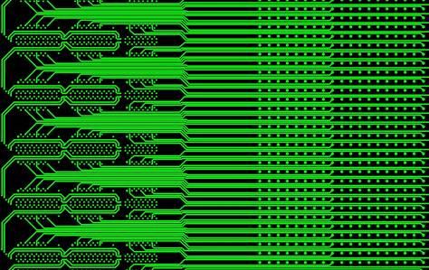
Parallel Routing Traces – Poor Design Practice
The example above of a parallel trace design is a poor practice.
However, broadside trace design is sometimes done on purpose and calculated into their PCB design. If you are not experienced with this type of design and it is not accounted for, we strongly recommend designing the traces perpendicular. The below image is of an intentional broadside design.
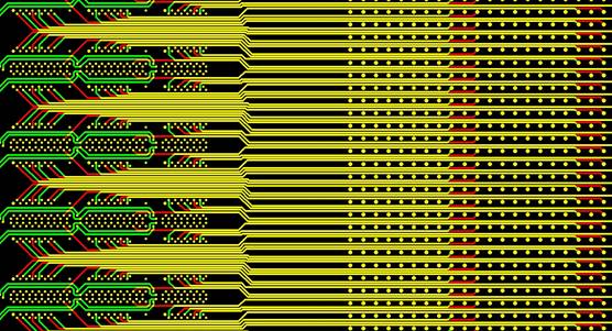
Broadside Routing Traces
Further development of your PCB design should follow a workflow that starts with a final schematic and follows these steps:
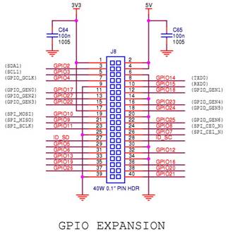
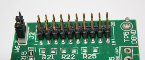
Example of an expansion header for connection to another PCB
Image Credit: Raspberry Pi Foundation)
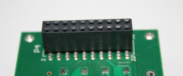
A common approach to connecting multiple boards is the stacking of boards on top of each other with connectors separating the boards. When designing for boards to be stacked, the substrate needs to be planned carefully to reduce impedance discontinuities, signal coupling and excessive electromagnet emissions.
All signal layers should be adjacent and closely coupled to an uninterrupted reference plane.
Closely coupled planes reduce AC impedance at the top end and dramatically reduce electromagnetic radiation. Radiation is further reduced by routing high-speed signals between the planes.
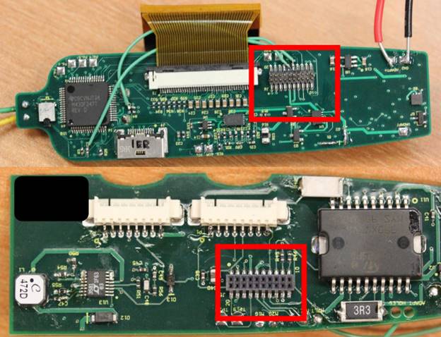
Stacked Circuit Boards– Male/Female Connectors for the Interconnect are Highlighted in the Red Boxes
Throughout the design workflow, be sure to consider how to integrate testing into your overall product production plan. Boards that are connected will need additional and more sophisticated testing to ensure signal strength and other operational specifications are met. It's much easier to incorporate this as the design proceeds than to go back when you are finished.
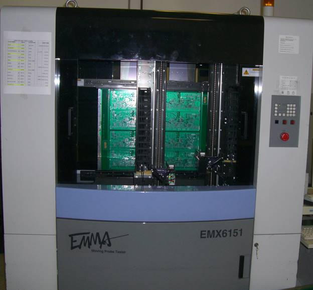
Flying Probe Test
What are the parameters that need to be addressed in testing?
Generally speaking, any high speed signals or traces sensitive to noise should be tested. Some examples are serial interfaces (SPI, I2C, UART, etc.), analog signals such as pre-amplified sensor measurements, audio signals, and high power traces that could have voltage drop, depending on how much current is flowing and if there's enough copper on the traces and connector pins.
ATG Flying Probe Test for Bare Boards
Taking the manufacturing process into consideration during the design phase will be important for the future repeatable construction of the final product as well as how to possibly service the product in the event of a failure.
Designing for manufacturing typically means incorporating test points into the overall design. Test points are commonly placed at the edge of the board to allow for probes to be easily connected to the circuit for assessing voltage.
Depending on your design, you may want a simple bare board test or more complex functional test while the board is energized. The board house could have the capability of having flying probes and programming it with the location of your test point pads.
Microcraft Flying Probe Test for Bare PCBs
Designing for future serviceability is an important factor to consider as you may need to troubleshoot or repair a product after it has been used and perhaps broken or otherwise become non-functional.
It will be important to design a mechanism for probing the entire assembly while the boards are connected, such as using a flex cable between multiple boards. With the cable harness replacing a straight pin-type, rigid connection, you can flip the boards over and have much easier access to probe while energized.
High speed design interconnectivity, such as clock signals and triggers for communication interfaces, requires specific considerations to ensure system performance, particularly in low-power environments. Steps need to be taken to minimize cross talk and excess noise generation, among other factors.
Impedance matching is also important as it maximizes power transfer and minimizes signal reflection at high speeds. At high speeds, a signal from a low-impedance source being transferred to a high-impedance source will flip its phase 180 degrees back and forth without proper termination of each end.
Here's a tip: For high speed SPI communication you will want to consider adding in-line resistors or buffers before connecting to an external board. The resistance you use is directly related to your PCB trace impedance. Using too little will consume a lot of current. Using too much resistance will have little to no effect on improving your signal transfer.
In-Line Resistors Before an Off-Board Connection
For high speed signals, it helps to have a ground in-between every other pin on the connector (for example, pin 1 = power, pin 3 = trigger 1, pin 5 = trigger 2, pin 7 = trigger 3 and pins 2, 4, 6, and 8 are all ground). This helps with reducing inductive coupling and cross talk.
That's some of the tried and true tips and considerations when designing for effective interconnectivity of PCBs. At the outset, keep in mind the overall product goal and market. Starting with good design software, work through a workflow that takes key design, test, manufacturing and servicing into consideration before your first board is spun.
There are a number of avenues for you to take when researching the various components you will need to assemble your circuit board as defined by your design. Of course, the internet has a wealth of information but can be overwhelming when trying to fight through marketing jargon.
Meeting with manufacturer representatives can be a good way to learn what’s new but, again, you are up against a sales person who, in the end, is trying to get you to buy a product. However, a manufacturer that is willing to share expertise and provide you with insight into industry standards, past experiences and samples can be a great resource.
Take your intricate PCB design concept from layout to manufacturing & assembly.
Complex circuit board projects with quality controls from start to finish and excellent technical engineering support are the core values that comes from partnering with San Francisco Circuits for your next project - from flex PCB to bare circuit boards, we are your one-stop shop for advanced technologies and prototypes.
Or EMAIL US to discuss & quote your project
Before you start researching components, be sure that you refer back to the original market research, product plan and operational requirements to help guide your selection criteria. Step away from the minutia of the circuit layout and go back to your overall product goal to determine the attributes and place in the market you are aiming for.
If you are aiming for a user-friendly product, you may want to pay more attention to the user controls/interface components. A high target price product will dictate a far different mix of components than a product aimed at the lower end of the market. Both of these divergent goals create different challenges to come within the target per unit price.
The per-unit target price for the finished product will dictate your overall parts budget. You’ll need to determine where to spend your available budget; there are some areas you won’t want to compromise on price (such as high speed, high reliability, and more sensitive devices) and others where you can save money (such as low-complexity and lower-quality mass produced consumer-based products.)
Here are some of the common components used to connect boards and how you should approach them for the best results:
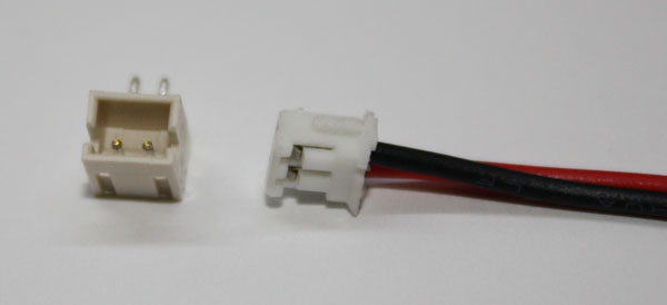
Copper Pins: ZH series connector (with mating plug) with power rating of 1A per pin
Note: For high current applications, this would be a poor choice for a connector.
The amount of power that a thin copper pin can handle is surprisingly little and can quickly become an issue if you are driving high power in a compact design. This is particularly the case in any instance that involves motors, solenoids or bright LEDs and may require multiple pins to achieve the required power rating on a connection.
In general, you want to stay 30% below what is expected at peak.
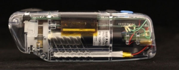
High-Powered Compact Design: Motorized Injector Medical Device with 2 Brushless DC Motor
Also note that voltage tends to drop over long, thin traces or thin pins that have a lot of resistance. Use too little copper in a high current trace, the resistance increases and creates a voltage drop across it. This can also affect a battery’s voltage output.
To combat this, use polygon pours for higher power traces. If board space is at a premium, add more copper per layer.
PCB with Multiple Polygon Pours:
The rectangular pour on the left was used for noise isolation and the others were used for high current traces
Transferring high-speed data between boards that have a modular design with several smart boards connecting USB, Ethernet and similar sources, you will have to account for application-specific connectors so you don’t mix signals.
For low speed transfers and less sensitive analog signals, use a combined connection to achieve desired results.
Combined Connections - Finished Receiver Mounted on PCBA
To further isolate and prevent coupling, double the amount of connector pins and place a ground in between each sensitive analog/digital signal.
First, a high yield output requires a manufacturing environment that is clean, precise and repeatable.
Ask your PCB manufacturer for examples of similar projects or any data that they can provide that proves adherence to quality controls. Depending on your application, you will need to test to specifications to meet the requirements of ISO, CE, IPC, IEC and others. These should be outlined in the market or product specification plans.
Boards should be assembled so that connections are straight and flat. Mechanical connections need to be secure and accurate to reduce stress on the components. Any board-to-board connectors that are even slightly mis-aligned can cause failures over time. Spend time making and testing prototypes to ensure the manufacturing process is performing to stated tolerances and can be repeated before starting your output.
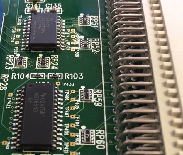
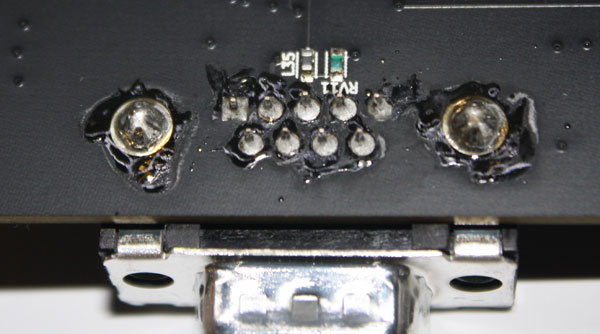
PCB Interconnect - Side A
There are two kinds of test points: a functional test point for when the board is energized and operating and a “flying probe test” where the board is populated but not energized to check analog components and shorts or open circuits. The functional test, while important in finding faults, is a more expensive route as it will require a detailed plan with operational requirements and established testing thresholds.
Test points are needed for large, complex and sensitive applications. To make this testing process easier, keep the functional testing front of mind in the design process. The design should accommodate test points in easy-to-probe places, such as near the edge of the board so they are more readily accessible. Another approach is to create a “test jib” with a cable assembly that interconnects two boards while exposing the test points. Boards can also be tested separately to ensure they meet individual specifications.
PCB Interconnect - Side B
Now that you have an assembled product, it’s time to put those test points in use to determine if the completed product is functioning to specifications.
Flying probe tests are common in post-assembly checks to make sure the right components were used and connections were made. This typically just calls for a test point report with schematic coordinates and bill of materials.
A functional test will measure voltage rails, rise/fall time on trigger lines, analog gains/sensitivities and much more. This will often require a specific testing fixture that utilizes interconnects or test points.
A common methodology is to test continuity between the boards. This is a good place to start since most problems occur here. Next, test all main power and voltage rails. Finally, test the signal integrity with an oscilloscope and tolerances for the main components versus the planned specifications.
Soldering should be automated for high density board applications to ensure connections are made optimally and completely. Flux residue from the soldering process can play a significant role in the performance of your board in terms of resistance. Board to board connections that have several through-hole pins need good flux cleaning since voltage can drop if there isn’t enough copper between connections with a high current path.
Using a solder wave pallet for stability in the soldering process can help ensure solid connections are made during assembly.
Flux Residue
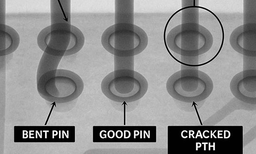
Shorts can occur on very high density connectors during the assembly process and need to be tested for during the quality control phase. Good board manufacturers will employ an X-ray machine to verify ball grid array packages.
Noise and inductive coupling issues are hard to trace during the functional test and remediate once a product is in production. As a preventative measure, start with a detailed test plan to lower the risk of these issues.
As an example, think of a board being used for a high-power heating application with a connection that extended to a heater and thermistor for feedback. The heater is Pulse Width Modulated at 100Hz with a varying duty cycles to control the average current through the heating element with power in the 10s of watts. What do you think the affect was on the connection? By examining the signal with an oscilloscope, you can locate power spikes on the thermistor.
Typically, the most common issue that can occur in a PCB interconnection is unintentional radiation and coupling of noise.
There are a few ways to find these issues. First, however, use shielding on connectors when dealing with sensitive and powerful signals. To determine if the signal integrity on an interconnection is bad, use an oscilloscope to find any noise or spikes caused by radiation. A near-field RF probe is the best tool to perform frequency sweeps to determine if a frequency tone is emitting from the connectors. This issue can also affect sensitive electronics nearby.
Near Field RF Probe
For example, a board being used for a high-power heating application with a connector that extended to a heater and thermistor was experiencing noise at the connection. By probing with an oscilloscope, you can find where the power spike is emanating from.
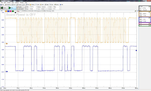
Oscilloscope Waveforms
Undoubtedly there is a lot to know and plan for when creating a PCB board that needs to connect to another board. But if you keep a few key suggestions in mind, the process can be less stressful and help see you through the process.
For your next PCB fabrication & assembly project, make sure to talk to the engineers at San Francisco Circuits to make your product concept a reality.
PCB School
Flying probe testing has been the golden standard of functional testing for low volume, prototype runs since the late 80s and 90s. It effectively flips the approach of the traditional in-circuit (ICT) bed-of-nails fixture test, where a custom-built frame with hundreds of spring-loaded pins contact test points simultaneously.
PCB School
Double-sided Ball Grid Array (BGA) assembly maximizes component density without increasing board size, enabling high-performance designs for applications ranging from smartphones and IoT devices to medical and industrial electronics.
PCB School
Managing strain during press-fit connector insertion is essential for high-density PCB reliability. Discover best practices and how San Francisco Circuits ensures reliable assembly for HDI, mil-spec, and medical applications.

PCB School
San Francisco Circuits covers the 8 types of PCB vias including blind, buried, microvias, through-hole, stacked, & thermal vias - what they are, how they work, & where they’re used in advanced PCB design.

PCB School
Discover why NIST 800-171 compliance is essential for PCB manufacturers. As a PCB buyer, learn how this cybersecurity framework safeguards your sensitive data & ensure you are engaged with a boardhouse that meets these requirements.
PCB School
San Francisco Circuits covers board-level tips for the design & layout of high-speed circuits in advanced applications.
