As is well known, designers are squeezing ever more performance out of printed circuit boards. Power densities are on the rise, and with them, high temperatures that can wreak havoc on conductors and dielectrics. Elevated temperatures - whether from I2R losses or environmental factors - affect thermal and electrical impedances, causing erratic system performance, if not outright failure. Differences in thermal expansion rates – a measure of the tendency of a material to expand when heated and shrink when cooled – between conductors and dielectrics generate mechanical stresses that cause cracking and connection failures, especially if the boards are subject to cyclic heating and cooling. If the temperature is high enough, the dielectric can lose its structural integrity altogether, knocking over the first domino in a cascade of trouble.
Heat-generation has always been a factor in PCB performance, and designers are accustomed to including heat sinks into their PCBs, but the demands of today’s high power-density designs frequently overwhelm traditional PCB heat-management practices.
Mitigating the effects of high temperatures have far-reaching implications, not just for the performance and reliability of high temperature PCBs, but also for such factors as:
A high temperature circuit board is typically defined as one with the Tg (glass transition temperature) greater than 170°C.
High temperature PCBs should follow a simple rule of thumb for continuous thermal load with an operating temperature ~25°C below the Tg.
So that means, if your product is in the range of 130°C or higher, a high Tg material is recommended.
The most common high Tg materials include:
- ISOLA IS410
- ISOLA IS420
- ISOLA G200
- Shengyi S1000-2
- ITEQ IT-180A
- ARLON 85N
In this article we’ll discuss some design methods and technologies used in high temperature PCB fabrication and PCB assembly to help the designer cope with high-temperature applications.
Partnering with an experienced PCB manufacturing and assembly provider with engineers that have worked with and modified multiple layouts in preparation for fabrication and assembly of electronic interconnects is crucial for complex projects.
Heat is dissipated through one or more mechanisms - radiation, convection, conduction – and the design team must keep all three in mind when deciding how to manage system and component temperatures.
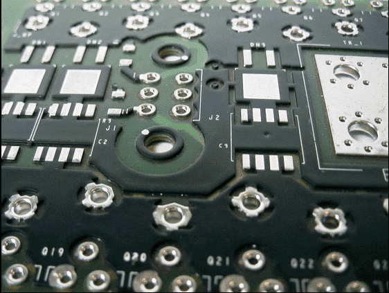
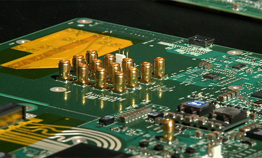
Heavy Copper PCB
Photo Credit: Robert Tarzwell
Radiation is the emission of energy in the form of electromagnetic waves. We tend to think of it as only in terms of things that glow, but the fact is that any object with a temperature above Absolute Zero radiates thermal energy. While it may be true that usually radiated heat is the least influential in circuit board performance, sometimes it can be the straw that breaks the camel’s back. To effectively remove heat, the electromagnetic waves should have a relatively clear path away from the source. Reflective surfaces frustrate the exodus of photons, causing significant numbers of them to redound on their source. If by unhappy chance the reflective surfaces conspire to form a parabolic-mirror effect, they can concentrate the radiated energies of a number of sources and focus it on one unlucky part of the system, causing real trouble. The key factors affecting thermal radiation are the temperature of the source (in absolute units, raised to the fourth power), the thermal emissivity of the material involved, and the surface area available for radiation.
Convection is the transfer of heat to a fluid – air, water, and so forth. Some convection is “natural”: the fluid absorbs heat from a source, becomes less dense, rises away from the source to a heat sink, cools, becomes more dense, sinks back to the source, and the process repeats. (Recall the grade school “rain cycle”) Other convection is “forced” by a fan or pump. The key factors affecting convection are the temperature difference between the source and coolant, the ease with which the source transmits heat, the ease with which the coolant absorbs heat, the coolant’s flow rate, and the surface area over which the heat is transferred. Liquids absorb heat much more readily than gasses.
Conduction is the transfer of heat via direct contact between the heat source and the heat sink. In many ways it’s analogous to electrical current: the temperature difference between the source and sink is akin to voltage, the amount of heat transferred per unit time is akin to amperage, and the ease with which heat flows through a thermal conductor is akin to electrical conductance. In fact, the factors that make a good electrical conductor tend to make good thermal conductors as well because both represent forms of molecular or atomic motion. Copper and aluminum, for instance, are excellent conductors of heat and of electricity alike. Large conductor cross-sections improve conductivity for heat and electrons. And as is the case with electrical circuits, long, tortuous flow paths can seriously degrade a conductor’s effectiveness.
Typically the primary mechanism for removing heat from a circuit board is to conduct it to a suitable heat sink, where convection bears it to the environment. Some heat is wafted and radiated directly from the source, but usually the bulk is drawn away through specially designed channels called “heat vias” or “thermal vias.” PCB heat sinks are comparatively large, highly emissive, surfaces (often corrugated or finned to further increase surface area) bonded to conductive (e.g., copper or aluminum) backings, a highly labor-intensive process. PCB heat sinks also may be connected to the unit’s chassis to avail of its surface areas. Often fans are used to provide a flow of cooling air, which in extreme cases may itself be cooled in a gas-liquid heat exchanger.
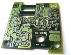
Multi Layer Thermal Board
Photo Credit: Robert Tarzwell
Boiling this down, the heat-management options available to a designer are to reduce power densities, remove or isolate the unit from heat sources, provide more powerful cooling mechanisms (e.g., bigger fans, liquid cooling systems, etc.), increase the size and accessibility of the heat sinks, use larger conductors, or use exotic materials capable of withstanding higher temperatures. All of these have implications for the cost, size, and weight of the total system that must be considered in the earliest concept-development and design stages.
PCB manufacturers are well aware of the limitations of standard fabrication practices, and strive to stay abreast of today’s design challenges by offering new kinds of PCBs designed specifically for high temperatures. These PCBs all employ heavy copper circuits to boost their current-carrying capacity while lowering I2R losses, but the way they accomplish it can vary considerably.
More and more we see “heavy copper” and “extreme copper” boards that, as the descriptions imply, use thicker, heavier copper layers than standard PCBs. If the heavy (or extreme) copper isn’t required everywhere, heavy copper circuits and standard copper circuits may be combined to allow power currents and signal currents to be carried on a single board.
The process for fabricating heavy/extreme copper PCBs is similar to that for standard PCBs, except for special etching and plating techniques. The advantages are larger current-carrying capabilities, lower I2R losses, higher mechanical strength, the ability to incorporate such features as high-efficiency on-board heat sinks and on-board planar transformers, and reduced product size (owing to the ability to combine heavy and standard circuits on a single board). Relative costs are lower because on-board heat sinks don’t require the tedious manual fabrication of standard, bonded, heat sinks.
A different approach is to embed heavy rectangular copper wires in lieu of heavy/extreme copper plating. The advantages vis-á-vis standard PCBs are similar to heavy/extreme copper PCBs: ability to combine power currents and signal currents, reduced heat generation and improved heat dissipation, increased strength, elimination of connectors, reduced layers, smaller overall system volume. Some claim that a wire-embeddedboard is easier to solder than a thick-copper board, but that should be evaluated on a case-by-case basis.
Another heat-management technology that should be considered is computational fluid dynamics (CFD) software that can be integrated with standard PCB design packages, such as Mentor Graphics’ FloTherm PCB®. As performance boundaries get pushed ever harder, old rules-of-thumb and back-of-a-napkin heat calculations become ever less reliable. In competent hands, a good CFD package – especially one that is specifically designed for PCB or electronic cooling applications – can eliminate a lot of guesswork, improve design efficiencies, obviate potentially costly errors, and reduce time to market.
With all the tradeoffs previously described, it’s essential that the product’s design and development be shaped by a team representing the key stakeholders: customers, sales, and marketing, of course, but also knowledgeable members of the customer-service, purchasing, manufacturing, and engineering departments. Suppliers, such as PCB manufacturers, with their design-for-manufacturing and technical expertise, must be integral members of the team; manufacturing, assembly, test, and service considerations must be built in, not added on.
Techniques such as Quality Function Deployment or TRIZ may be used to rank and reconcile competing design requirements, materials, and production techniques. First-pass cost-benefit analyses may be done parametrically then refined as real costs become available. To minimize roll-out problems, manufacturing and testing processes may be worked out, simulated, and refined with software such as Mentor Graphics’ “Valor MSS PCB” suite of solutions. The goal is frequent design iterations – creative failures, as they’ve come to be known – that rapidly converge to a final solution.
Although product requirements wax ever more exacting, we have the tools, technologies, and methodologies to cope with them. Survival in today’s hypercompetitive market requires that we adopt and adapt accordingly.
Or EMAIL US to discuss & quote your project
PCB School
Standards like MIL-PRF-55110, MIL-PRF-50884, and MIL-PRF-31032 exist to enforce reliability, traceability, and performance in environments where failure isn't acceptable.
PCB School
Flying probe testing has been the golden standard of functional testing for low volume, prototype runs since the late 80s and 90s. It effectively flips the approach of the traditional in-circuit (ICT) bed-of-nails fixture test, where a custom-built frame with hundreds of spring-loaded pins contact test points simultaneously.
PCB School
Double-sided Ball Grid Array (BGA) assembly maximizes component density without increasing board size, enabling high-performance designs for applications ranging from smartphones and IoT devices to medical and industrial electronics.
PCB School
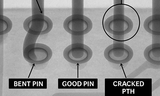
Managing strain during press-fit connector insertion is essential for high-density PCB reliability. Discover best practices and how San Francisco Circuits ensures reliable assembly for HDI, mil-spec, and medical applications.

PCB School
San Francisco Circuits covers the 8 types of PCB vias including blind, buried, microvias, through-hole, stacked, & thermal vias - what they are, how they work, & where they’re used in advanced PCB design.

PCB School
Discover why NIST 800-171 compliance is essential for PCB manufacturers. As a PCB buyer, learn how this cybersecurity framework safeguards your sensitive data & ensure you are engaged with a boardhouse that meets these requirements.
