Printed circuit boards, especially those used in PDAs (personal digital assistants) like cell phones, get a lot of abuse. In addition to collecting dust and dirt that penetrates the cases of cell phones, e-book readers and similar hand-held devices PCBs have been known to suffer from immersion in and splashing from liquids in day to day use. As a result, a service industry has emerged to provide cleaning and repair services for PCBs subjected to contaminants but not physical breakage in PDAs and larger devices.
NOTE: San Francisco Circuits does not perform Ultrasonic Cleaning or PCB cleaning services!
Partnering with an experienced PCB manufacturing and assembly provider with engineers that have worked with and modified multiple layouts in preparation for fabrication and assembly of electronic interconnects is crucial for complex projects.

Successfully taking your elaborate PCB designs from layout to PCB assembly is the core value that comes from partnering with San Francisco Circuits for your next project - from flex PCB to bare boards, we are your one-stop shop for intricate, advanced printed circuit technologies.
Cleaning a Printed Circuit Board (PCB) to service a high-use product is as delicate a process as is making the board. Connections can be damaged, components loosened and materials compromised if the wrong cleaning method is employed. To avoid these pitfalls, you need to take the same care in selecting the right cleaning method as you did when designing, specifying and producing the board in the first place.
What are those pitfalls and how can you avoid them?
Below we’ll explore the proven PCB cleaning options and some approaches you may want to be weary of.
There are a variety of contaminants that can accumulate on a PCB. Attacking the offending problem with the correct corresponding method will be more effective and efficient, and cause fewer headaches.
One of the most common occurrences is the accumulation of dirt or dust in or around the PCB. Gently using a small, delicate brush, such as a horsehair paint brush, can remove dirt and dust without affecting the components. There are limitations on where even the smallest brush can reach, such as beneath a component.
Compressed air can reach many areas but may damage vital connections, so it should be used with extreme care.
Specially designed vacuum cleaners for electronic components are also an option but cannot reach everywhere.
High temperature operations can cause some components that are coated in wax to become magnets for dust and dirt, causing tacky grime that cannot be removed with a brush or vacuum. Or a product gets a bath of sticky soda, making the board a gooey mess. Either way, these substances should be tackled before it builds up and affects performance.
Most grime can be removed with a cleaning agent, such as isopropyl alcohol (IPA) and a Q-tip, small brush or clean cotton cloth. Cleaning a PCB with a solvent like IPA should only be done in a well vented environment, ideally under a fume hood.
Demineralized water can be used as an alternative. Be sure to remove any excess moisture and properly dry the board (a few hours in a low-temperature oven can effectively remove any residual moisture.)
There are a number of commercially available PCB cleaning agents aside from IPA, ranging from acetone to chemicals made for cleaning electronics. Different cleaning agents can address specific types of contaminants, such as solder flux or wax. Keep in mind that harsh cleaning agents can remove component markings or cause damage to plastics or electrolytic capacitor jackets, or other exotic components like humidity sensors, so make sure you aren’t using a cleaning agent that is too strong. If you can, test the cleaner on an old component or connector you don’t need to be sure you don’t do more harm than good.
Ultrasonic cleaning machines use high-frequencies to cause cavitation; the violent implosion of billions of minute bubbles in the cleaning solution contained in an ultrasonic cleaner tank. The bubbles are created by transducers bonded to the bottom of the tank and excited to ultrasonic frequencies by generators. The implosion of these bubbles blasts away contaminants on the surface of parts being cleaned.
Ultrasonic can be defined as sound waves that have frequencies above the upper limit of the normal range of human hearing, which is about 20 kilohertz (20 kHz or 20,000 cycles per second). While that is true, ultrasonic cleaners when operating can be heard due to the action created by what we call ultrasonic cavitation.
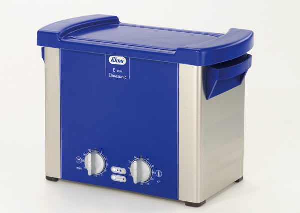
Benchtop Ultrasonic PCB Cleaner
This technique has lost some favor as a method for cleaning as it can cause damage to components or loosen connections, along with the dirt and grime. In fact, NASA has issued a directive that it no longer employs ultrasonic cleaning (page 31, section 7.1.4) as it can inadvertently cause separation of component end caps and actually cause damage to bond wires and bond wire pads internal to the IC via ultrasonic conduction of the ultrasonic energy via the integrated circuit lead-frame.
That being said, there is still a place for ultrasonic cleaning applications. The ultrasonic cleaning process can reach the most difficult, hard to reach places underneath high density components on most any parts of a circuit board. This is not the case for SMD devices that have small gaps that are smaller than the surface tension coefficient of the cleaning fluid. However, the process is fast and there are numerous high-capacity machines available to address high-volume cleaning needs.
Cavitation is not a gentle process. It has been calculated that temperatures in excess of 10,000°F and pressures in excess of 10,000 PSI are generated at the implosion sites of cavitation bubbles.
Measured in cycles per second, ultrasonic cleaners can produce from 25 kHz to 100+ kHz. Lower frequencies create larger cavitation bubbles compared to higher frequencies. Larger bubbles implode more vigorously and are used, for example, to remove gross contaminants from fabricated metal components. Higher frequencies create smaller bubbles that clean more gently but are better able to penetrate cracks, crevices and blind holes. The higher frequencies are used for cleaning highly polished or delicate surfaces.
There are companies that specialize in PCB cleaning. Note that we (San Francisco Circuits) do not provide PCB cleaning services! We are a high-end provider of PCB manufacturing and assembly.
Depending on your need - such as a high quantity of boards, what needs to be cleaned off and how delicate the board is - may send you in search of an outside source for your cleaning needs.
If you are constantly having issues with boards needing to be cleaned, there may be something more significant in the design or manufacturing process that needs to be examined. Our consulting engineers are able to help you pinpoint a problem and devise a long-term solution to better ensure PCBs remain clean and in operational tolerances.
Cleaning a PCB doesn’t have to be a daunting task. Keeping the above tips and advice in mind will help in ensuring get the cleaning job done right.
Or EMAIL US to discuss & quote your project
PCB School
Standards like MIL-PRF-55110, MIL-PRF-50884, and MIL-PRF-31032 exist to enforce reliability, traceability, and performance in environments where failure isn't acceptable.
PCB School
Flying probe testing has been the golden standard of functional testing for low volume, prototype runs since the late 80s and 90s. It effectively flips the approach of the traditional in-circuit (ICT) bed-of-nails fixture test, where a custom-built frame with hundreds of spring-loaded pins contact test points simultaneously.
PCB School
Double-sided Ball Grid Array (BGA) assembly maximizes component density without increasing board size, enabling high-performance designs for applications ranging from smartphones and IoT devices to medical and industrial electronics.
PCB School
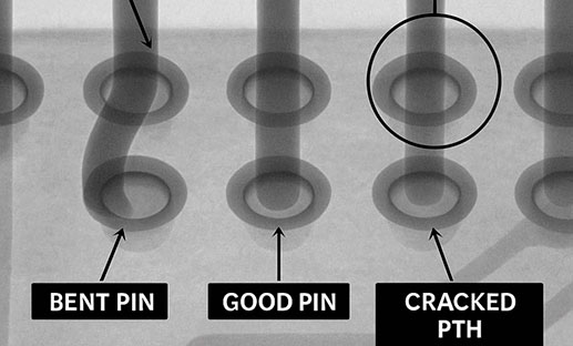
Managing strain during press-fit connector insertion is essential for high-density PCB reliability. Discover best practices and how San Francisco Circuits ensures reliable assembly for HDI, mil-spec, and medical applications.
PCB School
San Francisco Circuits covers the 8 types of PCB vias including blind, buried, microvias, through-hole, stacked, & thermal vias - what they are, how they work, & where they’re used in advanced PCB design.

PCB School
Discover why NIST 800-171 compliance is essential for PCB manufacturers. As a PCB buyer, learn how this cybersecurity framework safeguards your sensitive data & ensure you are engaged with a boardhouse that meets these requirements.
