
We'll help you avoid this.
Lack of knowledge in manufacturing and PCB manufacturing processes
The knowledge of the manufacturing process will impact the manufacturing and cost.
Minimal utilization of manufacturing capabilities (example with Impedance)
How impedance calculations by the manufacturer will impact the finished design, performance, turn time, cost.
Lack of knowledge in materials
How to choosing of correct materials will impact performance, turn time and cost.
Neglecting the suppliers support during design and layout
How the DFM report during preliminary stages will impact turn time & cost.
Unrealistic expectations
How a reality check will impact performance, turn time & cost.
30 minutes of education will almost eliminate these reasons and expand your knowledge. We will present this in a interesting and fun visual way. At a convenient time that you can choose a face to face or telephone conference.
No obligation for getting this PCB training session, complimentary of San Francisco Circuits
Our experts are available to consult 24/7. So, call us anytime at 650.655.7202.
The same great SFC customer service
The same great attention to detail
The same great ease of doing business
AT GREAT OFF SHORE PRICES
CALL US TODAY TO LEARN MORE ABOUT IT.
SPECIAL 15% OFF YOUR FIRST ORDER
Select San Francisco Circuits for your offshore PCB fabrication choice
P: +1.650.655.7203
M: +1.408.449.6788
.jpg)
Andrew Gonzales' background is primarily in front end planning. He has extensive experience in front end planning including extensive experience in the front end engineering and planning including comprehensive DFM analysis, interacting with customers on any technical level.
"Our job is to make sure the customer is getting exactly what he wants"
"It is my job to Consult with customers on all aspects of PCB manufacturing starting with the very beginning stages of design, manufacturing and assembly. Including providing customers with the reference documentation, specs, and whatever it takes to make sure that everything is right. Our job is to make sure the customer is getting exactly what he wants."
When asked what he feels is the most important part of this job, Andrew states, "always being available and always having an answer. In today's work environment, I feel that people want to do business with someone they can rely on and be available all the time and always have an intelligent answer."
When not at work at San Francisco Circuits Andrew enjoys people. He said recently, "I am very much a people person so I like to get out in the world and do things with people or where I can meet people. Activities like snowboarding, hiking, biking that help me work up an appetite so I can go out to a nice dinner or lunch with friends & family or coworkers and customers."
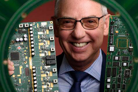
"San Francisco Circuits CEO Alex Danovich was interviewed by CompanyWeek, a publication from parent company Sustainment that highlights stories from American manufacturers."
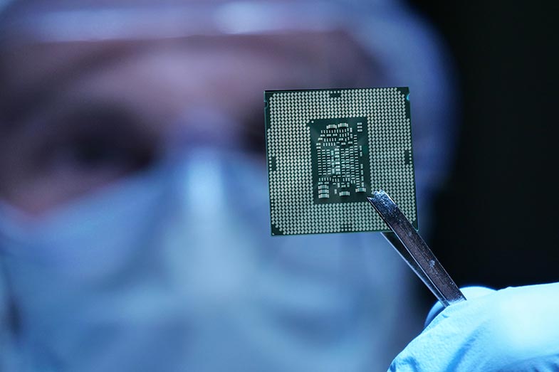
"The global integrated circuits / chip shortage has impacted many industries across the globe, and though it does seem to slowly be getting better, we’re still a ways out from things stabilizing and turning back to normal."

"We are pleased to announce we have achieved NIST 800-171 compliance–meaning we are able to protect sensitive government data and information following federal guidelines from the National Institute of Standards and Technology (NIST) "
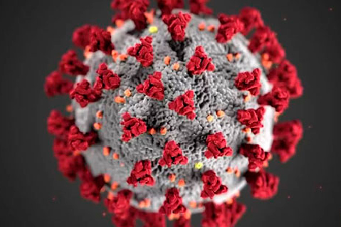
"The Health Officers of the Counties of San Francisco, Santa Clara, San Mateo, Marin, Contra Costa and Alameda have made an announcement that would impact our day-to-day work. Here’s information you need to know that could affect you."
"San Francisco Circuits is honored to have been chosen as the top PCB supplier in the industry and featured on an episode of National Television's "World's Greatest!" View the video here."
"New office, new staff - same great technology. We opened our second location in sunny San Diego on February 1st. We're excited to now have two offices that work tirelessly to meet your needs."
