The purpose of the PCB school is to help educate engineers, technicians and buyers on printed circuit boards.
Our team of experts in the PCB industries have been proudly educating other printed circuit professionals since 2005. With this section, we hope to provide the opportunity to gain a comprehensive grasp of concepts in a shorter period of time, to remain up to date in the field, and/or to acquire the technical knowledge to begin or advance their skills.
We offer access to knowledge to everyone who needs them and wants to learn the technologies available in PCB design, PCB fabrication and PCB assembly.

PCB School
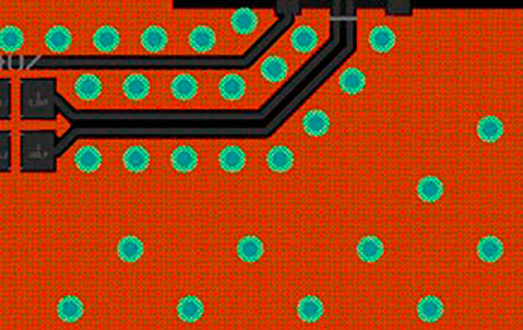
San Francisco Circuits covers the 8 types of PCB vias including blind, buried, microvias, through-hole, stacked, & thermal vias - what they are, how they work, & where they’re used in advanced PCB design.

PCB School
Discover why NIST 800-171 compliance is essential for PCB manufacturers. As a PCB buyer, learn how this cybersecurity framework safeguards your sensitive data & ensure you are engaged with a boardhouse that meets these requirements.
PCB School
San Francisco Circuits covers board-level tips for the design & layout of high-speed circuits in advanced applications.

PCB School
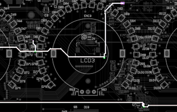
PCB line tracing relates to both function and safety in circuitry. We discuss the significance of careful line tracing through both clearance and creepage.

PCB School
Via tenting is the application of soldermask to encase or seal the via’s opening. A via is essentially a hole drilled into the PCB that facilitates connections between multiple PCB layers. An untented via, on the other hand, remains uncovered by a soldermask layer. The decision to expose or cover these vias carries both advantages and disadvantages contingent upon your specific design and manufacturing requirements.
PCB School
The Essential Guide to PCB Assembly Drawings: Understanding Polarities, Pin1 Marking & Anode/Cathode Markings. Learn more about understanding the XY File, component locations, & polarized component orientations.
PCB School
This article explores insertion loss: its properties, how loss occurs throughout a signal path in a system, and things we can do to minimize it.
PCB School
There are a number of factors to consider with the mechanical aspects of a PCB. In this article, we are going to dive into the various ways a PCB designer can help to deliver a board meeting mechanical and thermal requirements while staying competitive on cost.
Unnecessarily tight constraints on the board will be a cost driver. Meanwhile, an insufficient set of physical parameters leaves the potential for a board that does not meet the necessary requirements in the field.
One's goal is to find the sweet spot between precision and price. Believe it or not, that is possible to do.
PCB School
At what point is a load considered high voltage or high current, and what does that mean for the PCB design process? There are several factors that must be considered when specifying components and laying out a PCB for these kinds of conditions. Here's what you need to know to properly manage copper pads, copper traces, an copper planes.
PCB School
Is Serpentine Routing a good choice for your next PCB project? Signal integrity is very important in digital and analog systems. The routing of your PCB plays an important role in helping to increase performance by keeping signals in sync. A few minor disasters in your routing can lead to a major disaster. Learn more about why serpentine routing may be the right choice for you.
PCB School
As new electronic devices are developed and more features need to be added, the space on a PCB becomes even more important. And as devices need to be smaller and smaller due to consumer demand, PCBs have to be dense to fit all the components. Which is why proper use of microelectronics best-practices in PCB production (design/layout, fabrication & PCB assembly) ensures devices function well even with reduced form factors.
PCB School
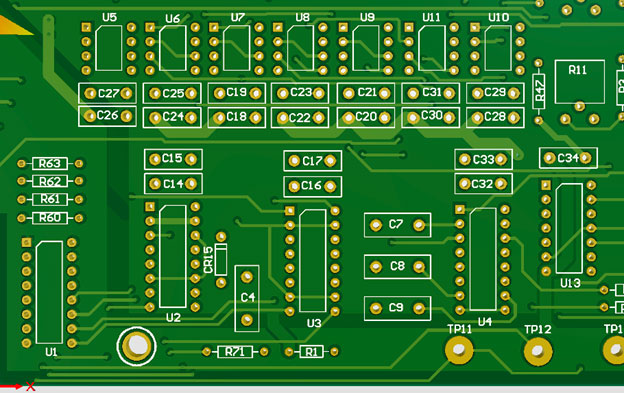
As the name suggests, a PCB layout is how the components are laid out on a printed circuit board. There’s no right or wrong way to design the layout as it depends on the intended purpose of the end product.
However, if the PCB layout is not handled correctly, the end product will not be effective, affecting time and your bottom line. A few of the main things to consider for a PCB layout are the orientation of components, part size, and how and where components are placed in relation to each other.
PCB School
There are several factors that drive trace width, length, and style during the PCB design process of your next PCB prototype. This article will dive into a variety of applications that demand specific trace layout characteristics and how or when to incorporate them into your PCB design.
PCB School
How do you save space in a PCB design? Pogo-Pin interfaces allow you to remove unnecessary space and save money in your PCB designs. The basic benefit of Pogo-Pins allow you to convert bulky header-based connections to smaller, zero-profile connections that free up board space and reduce cost. A variety of individual pogo pins exist today as an off-the-shelf solution for both cable or Printed Circuit Board (PCB) integrations. Learn more tips in this article.
PCB School
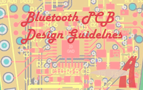
Incorporating Bluetooth technology into a PCB design requires various considerations. Check out some Bluetooth circuit design tips here.
PCB School
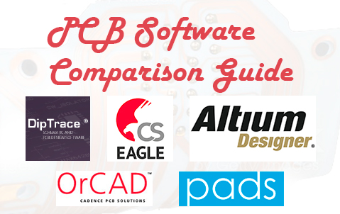
Our ultimate guide to PCB design software comprehensively compares the top 6 PCB CAD programs available and includes a step-by-step tutorial of the top 3 final programs. This 6,000+ word guide compares DipTrace, EagleCAD, KiCAD, PADS, OrCAD and Altium Designer.

PCB School
A multiple board PCB attached through electronic interconnects will pose a difficult, complex challenge for your engineers in layout. You can make working with electronic interconnects and multi-board assemblies easier! Find design considerations and principles in this article.
PCB School
Heat-generation has always been a factor in PCB performance with demands of today’s high power-density designs frequently overwhelming traditional PCB heat-management practices. This article will discuss some design methods and PCB technologies used to help the designer deal with high-temperature applications.

PCB School
Cleaning a Printed Circuit Board (PCB) to service a high-use product is as delicate a process as is making the board. Explore the options to cleaning PCBs here, ranging from dry cleaners like brushes, compressed air and vacuum cleaners to wet cleaners including demineralized water and isopropyl alcohol. We also include a special section on Ultrasonic PCB cleaning with a warning from NASA on the use of ultrasonic cleaning.

PCB School
This PDF gives a detailed introduction to flexible circuitry's uses, materials, characteristics and more.
Check out a preview of SFC's Intro to Flex Circuits
PCB School
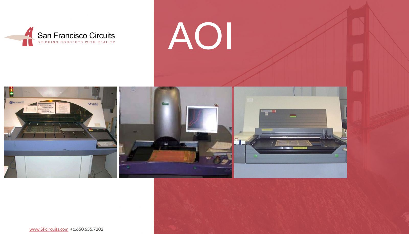
In this issue, we look at all the equipment needed to manufacture PCBs including equipment for:
|
|
| Check out a preview of SFC's PCB Manufacturing Equipment | |
PCB School
This beginner's article on high precision PCB drilling discusses the ongoing miniaturizations of electronics and the increased demand for high-density vias and through holes for interconnects. High precision drilling through mechanical and laser drilling produce these high density boards.
