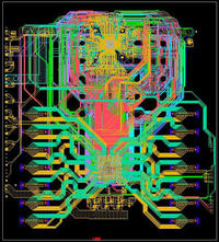
16 layer PCB
with blind and buried vias
Disclaimer: San Francisco Circuits does not provide either PCB design or PCB layout services. San Francisco Circuits provides PCB fabrication and PCB assembly services. Use our simple PCB stackup designer tool to help you design and visualize your own multilayer PCB stackup from 4 to 14 layers
As the name suggests, a PCB layout is how the components are laid out on a printed circuit board. There’s no right or wrong way to design the layout as it depends on the intended purpose of the end product.
However, if the PCB layout is not handled correctly, the end product will not be effective, affecting time and your bottom line. A few of the main things to consider for a PCB layout are the orientation of components, part size, and how and where components are placed in relation to each other.
When you place a PCB fabrication / assembly order with us, our engineering experts will ensure these layout considerations don’t violate any specifications for fabrication and assembly.
In almost all cases, the starting point for designing a PCB layout is schematic creation.
A schematic serves as the blueprint for component placement on an assembled PCB. And, it also makes the design process easier because it indicates where wires go and the other parts of the design footprint.
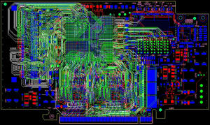
8 Layer HS DDR PCB Design
The next step is to optimize the PCB design for optimal performance. For example, it’s important to keep similar components grouped together in the proper way to reduce electromagnetic interference and noise. And, to keep traces shorter in the PCB, it’s important to make sure the different sections of a circuit are arranged as linearly as possible.
And finally, choosing the right PCB shape and size, user interface, and PCB substrate are also important. There’s a lot to think about when you design a PCB layout, and one small mistake could create massive issues in the end project resulting in lost time and money.
Our veteran engineering team will take your PCB layout from concept to reality – no matter how complex.
Our production and technology capabilities include RF PCB manufacturing, rigid / rigid-flex / flex, metal core, and more - covering a wide range of PCB surface finishes.
San Francisco Circuits expertise truly lies in prototype PCB services. We can assist with boards from simple two-layer PCB designs to more complex, high-density, 30+ layer PCBs.
Find out why we are the ideal solution for any project size.
Get a PCB quote from us today to see how we can help you from PCB layout to final product.
