Here are some PCB horror stories that gave us the chills:

An engineer came to us and said that they trusted someone else with their crucial project. The net list was supplied with the data but was not compared to the gerbers. They were "Shocked" when the boards had a power to ground short.
Our customer had to attend a trade show to present their new design. They had 1 week to get the board done. They ordered the boards on a 3 day turn but didn't receive the boards until after the trade show! What's just as bad, the supplier never responded when they asked for status.
Avoid your own PCB horror story, contact our PCB professionals at 800-SFC-5143 or email sales at sfcircuits dot com and discuss what you're trying to accomplish with your PCBs.
Get professional advice on material selection, stack-up, copper weight, final finish, filled vias, stacked vias, blind and buried vias, drill to copper requirements and much more for all your PCB fabrication and assembly needs.
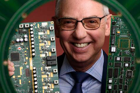
"San Francisco Circuits CEO Alex Danovich was interviewed by CompanyWeek, a publication from parent company Sustainment that highlights stories from American manufacturers."
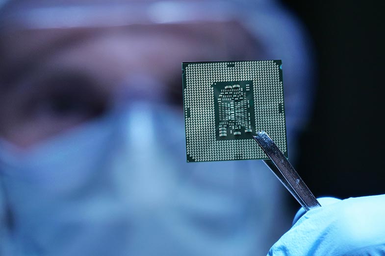
"The global integrated circuits / chip shortage has impacted many industries across the globe, and though it does seem to slowly be getting better, we’re still a ways out from things stabilizing and turning back to normal."

"We are pleased to announce we have achieved NIST 800-171 compliance–meaning we are able to protect sensitive government data and information following federal guidelines from the National Institute of Standards and Technology (NIST) "
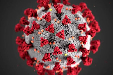
"The Health Officers of the Counties of San Francisco, Santa Clara, San Mateo, Marin, Contra Costa and Alameda have made an announcement that would impact our day-to-day work. Here’s information you need to know that could affect you."
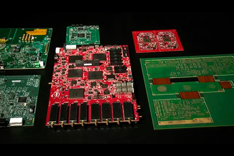
"San Francisco Circuits is honored to have been chosen as the top PCB supplier in the industry and featured on an episode of National Television's "World's Greatest!" View the video here."

"New office, new staff - same great technology. We opened our second location in sunny San Diego on February 1st. We're excited to now have two offices that work tirelessly to meet your needs."
