How do you reduce the cost of your board and make the PCB fabrication and assembly process painless?
The answer is ensuring manufacturability through design for manufacturability (DFM). DFM set design guidelines that take into account the processes and capabilities of the manufacturing industry.
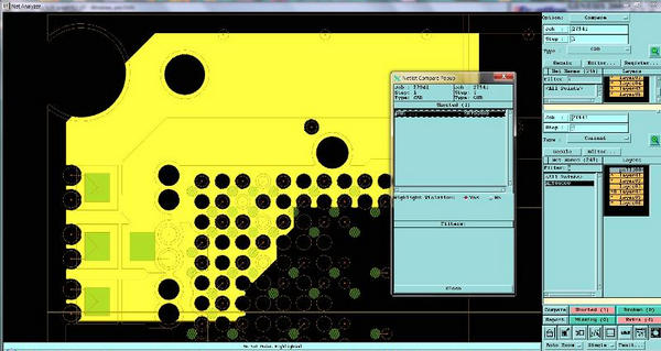
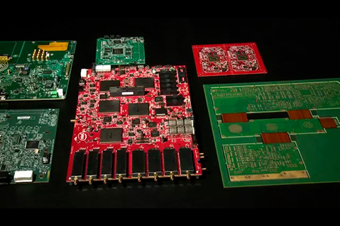
Net List GUI - Compare
Designing your boards without preliminary discussion of what you're trying to accomplish with your PCB supplier.
There are so many different PCB materials available today that some of them are not readily available and others are more available. Flex, high speed, RF, high temp & RoHS boards can all have different materials and each material can be made by a different manufacturer with slightly different specifications. Lead time on some special materials can be several weeks. You will want to choose the material that fits your needs more closely and is more available.
Designing your boards without detailed stack up information from fabricators.
Every manufacturing facility has different manufacturing tolerances that can affect the target impedance and/or stack up. When you design your board without consulting with your PCB suppliers, adjustments may need to be made in order to certify your impedance requirements. This may increase the lead time and the cost, if special order material is necessary to make the adjustments. Have the stack up provided by your PCB suppliers before proceeding with your design.
For help planning your own multi-layer stackup, use our free PCB Stackup / Design tool and read our PCB Stack-Up Guide for more information on this important topic.
Setting up the plane layers with the same requirements as signal layers.
This can add unnecessary difficulty to your printed circuit board and cause potential yield issues, increasing the cost of the boards as a result.
Your data package does not include an IPC-356A net list.
The IPC-356A net list allows your PCB supplier to find errors in the PCB design by comparing the gerbers to the CAD database. It's possible that the files contained errors or were corrupted when exported. Without this net list, many of the errors cannot be caught.
In order to achieve the best results with your PCB, contact our PCB professionals by calling 800-SFC-5143 and discuss what you're trying to accomplish with your PCB.
Get professional advice on the technology that you require to manufacture your PCB, in the most economical way. You will get advice based on material, stack up, copper weight, final finish, filled vias, stack vias, blind and buried vias, drill to copper requirements and much more...
Read more about our PCB production capabilities and our PCB assembly capabilities.
"San Francisco Circuits CEO Alex Danovich was interviewed by CompanyWeek, a publication from parent company Sustainment that highlights stories from American manufacturers."
"The global integrated circuits / chip shortage has impacted many industries across the globe, and though it does seem to slowly be getting better, we’re still a ways out from things stabilizing and turning back to normal."

"We are pleased to announce we have achieved NIST 800-171 compliance–meaning we are able to protect sensitive government data and information following federal guidelines from the National Institute of Standards and Technology (NIST) "

"The Health Officers of the Counties of San Francisco, Santa Clara, San Mateo, Marin, Contra Costa and Alameda have made an announcement that would impact our day-to-day work. Here’s information you need to know that could affect you."
"San Francisco Circuits is honored to have been chosen as the top PCB supplier in the industry and featured on an episode of National Television's "World's Greatest!" View the video here."
"New office, new staff - same great technology. We opened our second location in sunny San Diego on February 1st. We're excited to now have two offices that work tirelessly to meet your needs."
