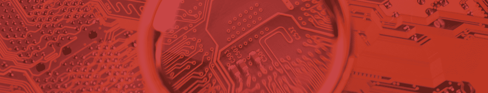
It's common practice to have wave solder or hand assembly for through-hole on standard technology. But how do we handle through-hole assembly when a printed circuit board (PCB) has Ball Grid Array (BGA) components on both sides, dense boards, or through-hole components that are very close to Surface-Mount Technology (SMT) parts? Hand soldering can have inconsistencies and wave solder might not be an option due to high costs of wave solder fixtures.
Automated selective solder will be the best solution for these technologies. This is the best way to assemble through hole components and get consistent high quality assembly that meets Class 3 requirements.
To learn more about selective solder assembly, contact us at sales [at] sfcircuits [dot] com or call 800-SFC-5143.
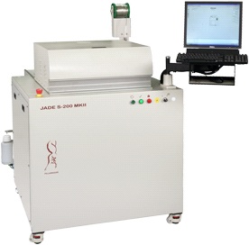
We offer additional PCB assembly solutions:
• Turnkey and Consigned Assembly
• Quick turn prototypes, as fast as 24 hours
• Commercial, Medical or ITAR requirements
• Production capabilities
• Box build
• High Technology Assembly, 01005 component size, POP - package on package and flip chip assembly
You can combine PCB fabrication and assembly services and save yourself time and money.
You will receive fully fabricated and assembled boards when you need them.
Call us today to get your project started. 1-800-SFC-5143
Issue #4 - Manufacturing Design Rules
Issue #5 - Quick turn Fabrication and Assembly
"San Francisco Circuits CEO Alex Danovich was interviewed by CompanyWeek, a publication from parent company Sustainment that highlights stories from American manufacturers."
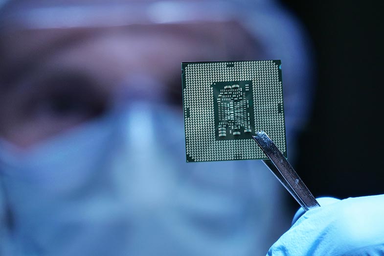
"The global integrated circuits / chip shortage has impacted many industries across the globe, and though it does seem to slowly be getting better, we’re still a ways out from things stabilizing and turning back to normal."

"We are pleased to announce we have achieved NIST 800-171 compliance–meaning we are able to protect sensitive government data and information following federal guidelines from the National Institute of Standards and Technology (NIST) "
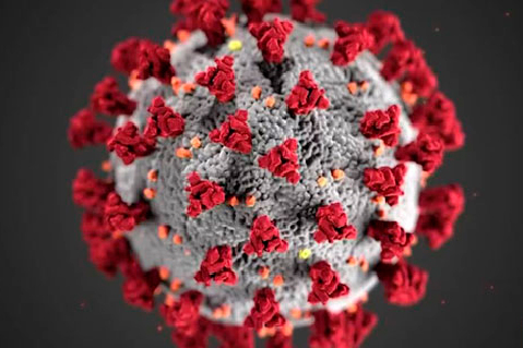
"The Health Officers of the Counties of San Francisco, Santa Clara, San Mateo, Marin, Contra Costa and Alameda have made an announcement that would impact our day-to-day work. Here’s information you need to know that could affect you."
"San Francisco Circuits is honored to have been chosen as the top PCB supplier in the industry and featured on an episode of National Television's "World's Greatest!" View the video here."
"New office, new staff - same great technology. We opened our second location in sunny San Diego on February 1st. We're excited to now have two offices that work tirelessly to meet your needs."
