A PCB surface finish is crucial for a printed circuit board as it prevents the copper (exposed traces, pads, holes and ground plains) from oxidation – a critical ingredient to high-level application performance.
A surface finish is essential for making a reliable connection between the PCB and the electronic component. A surface finish has two major functions, to provide a solderable surface for sufficient soldering components to the PCB, and to protect any exposed copper from oxidizing.
When it comes to choosing the right type of final surface finish, it is just as important as selecting the right material for your bare board. Selecting the correct surface finish for your application is critical for performance. For assistance with selecting a surface finish, send our trusted engineers an email or call.
With increasing demands for thin, high-density, fast speeds, and lightweight applications, the solder finish will make all the difference.
Modern surface finishes are lead-free, in accordance with Restriction of Hazardous Substances (RoHS) and Waste Electrical and Electronic Equipment (WEEE) directives, and include:
Choosing the correct PCB surface finish for your application requires taking factors into account like cost, the final application environment (e.g. high-heat/thermal, vibration/stability, RF), component density/selection, lead/lead free requirements, shelf life, shock/drop resistance, production volume, and throughput.
Due to the increased demand for improved performance of electronic applications, surface finishes have also been upgrading. Because of tighter PCB topography the HASL surface finish is quickly being replaced by gold-based surface finishes like ENIG, ENEPIG, and soft/hard gold. The gold-based surface finishes have a lot to offer in terms of features and benefits when used in applications.
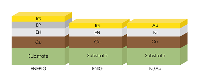
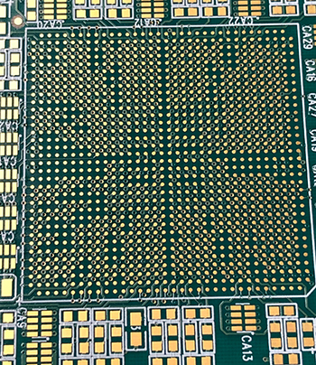
ENIG consists of two layers of metallic coating, which are deposited on the copper surface through chemical process, 2-5μ inches of immersion Gold (Au) over 120-240μ inches of electroless Nickel (Ni).
The nickel layer protects the copper from oxidation, and the gold layer protects the nickel layer. This dramatically increases the resistance to corrosion and also maintains a flat surface which is crucial for assembly of leadless components. ENIG usage has become very common now due to the accountability for lead-free regulations.
| ENIG (Electroless Nickel Immersion Gold) |
|---|
| PROS |
| Flat Surface - Excellent for Assembly of Dense Topography PCBs |
| Long Shelf Life |
| Great for Plated Holes and Fine Pitch / BGA / Small Components |
| Wire Bondable (When Aluminum Wire Is Used) |
| CONS |
|
Expensive |
| Significant Signal Loss |
| Unable to Rework |
| Black Pad / Black Nickel |
| Not Suitable for Touch Contact Pads |
| MOST COMMON USES |
| High Density PCBs |
| Rigid PCBs |
| Flex PCBs |
| Industries: Consumer, Data/Telecom, Aerospace, Military, High Performance, and Medical |
| Properties of ENIG | |
|---|---|
| Properties | ENIG |
|
Contact Applications |
Yes |
|
Deposit |
Immersion |
|
Exposed Copper |
No |
|
Handling |
Normal |
|
Process Control |
Fair |
|
Process Cost |
Medium |
|
Required Thermal Cycles |
>2 |
|
Shelf Life |
Long (1+ Years) |
|
SMT |
Flat |
|
Thickness |
3 - 10 µin of Gold over |
|
Thin Board Finish |
Yes |
| Applications of ENIG | |
|---|---|
| Applications | ENIG |
|
BGA & μBGA |
Yes |
|
Contact/Connector |
Yes |
|
Fine Pitch SMT |
Yes |
|
Flip Chip |
Yes |
|
High Reliability |
High |
|
RoHS Compliant |
Yes |
|
Solder Joint Integrity |
Good |
|
Wire Bonding |
Yes (Al) |
ENEPIG is probably not new to you, but it is a surface finish that has become increasingly popular recently due to the price reductions in palladium. It also has increased in popularity and use because of its many features and benefits. It also has a distinct advantage over the ENIG surface finish, which we’ll get into below.
The ENEPIG surface finish is composed of four metal layers:

The difference between ENEPIG and ENIG is the added layer of palladium. The palladium helps protect the nickel layer from corrosion, which helps prevent “black pad” from occurring. This is one of the distinct advantages of ENEPIG over the ENIG surface finish. The immersion gold layer that sits atop the palladium offers nearly-complete board protection by protecting and preserving the palladium underneath.
When compared to other surface finishes, like hard gold and soft gold plating, ENEPIG has become more affordable in recent years. The cost of the ENEPIG surface finish decreased because the added palladium layer reduces the required thickness of the more expensive gold layer.
The ENEPIG finish is capable of the majority of the ultra-demanding requirements with multiple package types like through-holes, SMT, BGA, wire bonding, and even press fit.
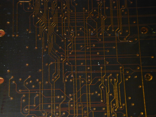
The PCB surface finish with ENEPIG is very thin (between 0.05μm and 0.1μm), making the assembly and soldering process very simple and definitely more reliable when compared to ENIG. ENEPIG also has a long shelf life due to its durability and resistance from tarnishing.
| ENEPIG (Electroless Nickel Electroless Palladium Immersion Gold) | ||
|---|---|---|
| PROS | ||
|
Black Pad Free |
||
|
Good for Touch Contact / Push Contact |
||
|
Higher Reliability Wire Bonding than ENIG |
||
|
Stronger Solder Reliability than ENIG |
||
|
Cheaper than Electrolytic Gold |
||
|
Lead Free & RoHS Compliant |
||
|
Long Shelf Life |
||
|
Multiple Reflow Soldering Capability |
||
|
Flat Surface - Excellent for Solderability |
||
|
Great for Plated Holes and Fine Pitch / BGA / Small Components |
||
|
Easier Inspections |
||
| CONS | ||
|
More Expensive than ENIG |
||
|
May Not Be As Reliable for Gold Wire Bonding When Compared to Soft Gold |
||
| MOST COMMON USES | ||
|
Multi-Layer PCBs |
||
|
Mixed Package Technologies |
||
|
Industries: Military, Medical, Aerospace, High Performance Devices |
||
| Properties of ENIG | |
|---|---|
| Properties | ENEPIG |
|
Contact Applications |
Yes |
|
Deposit |
Immersion |
|
Exposed Copper |
No |
|
Handling |
Normal |
|
Process Control |
Fair |
|
Process Cost |
High |
|
Required Thermal Cycles |
>2 |
|
Shelf Life |
Long (1+ Years) |
|
SMT |
Flat |
|
Thickness |
1 - 2 µin of Gold over 4 - |
|
Thin Board Finish |
Yes |
| Applications of ENEPIG | |
|---|---|
| Applications | ENEPIG |
|
BGA & μBGA |
Yes |
|
Contact/Connector |
Yes |
|
Fine Pitch SMT |
Yes |
|
Flip Chip |
Yes |
|
High Reliability |
High |
|
RoHS Compliant |
Yes |
|
Solder Joint Integrity |
Good |
|
Wire Bonding |
Yes |
Depending on applications, printed circuit board technologies use gold extensively. Gold has good electrical conductivity, tarnish resistance, solderability after storage, and being excellent etch resist.
Electrolytic Ni/Au has a layer of gold plating over a base of electroplated nickel. The purity of the gold plating categorizes this finish as either hard gold (99.6% purity) or soft gold (99.9% purity). The choice of hard gold versus soft gold depends on the type of application you are looking to create
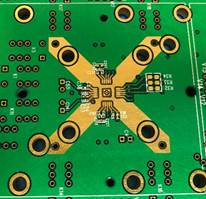
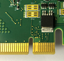
Hard gold is a gold alloy with complexes of cobalt, nickel or iron. A low-stress nickel is used between gold over-plating and copper. Hard gold is not suitable for wire bonding.
We recommend using the hard gold surface finish for components and applications with heavy usage and a high likelihood of wear and tear, like:
The thickness of the hard gold surface finish will vary depending on the applications. When hard gold is used for compliance in military applications, the minimum thickness shall be 50 -100 micro inch.
Nonmilitary applications require 25 to 50 micro inches. Here are the recommended minimum and maximum thickness values:
| Properties of Hard Gold | |
|---|---|
| Properties | Hard Gold |
|
Contact Applications |
Yes |
|
Deposit |
Electrolytic |
|
Exposed Copper |
Yes |
|
Handling |
Normal |
|
Process Control |
Fair |
|
Process Cost |
High |
|
Required Thermal Cycles |
>2 |
|
Shelf Life |
Long (1+ Years) |
|
SMT |
Flat |
|
Thickness |
98% Pure, 23 Karat 30 - |
|
Thin Board Finish |
Yes |
| Applications of Hard Gold | |
|---|---|
| Applications | Hard Gold |
|
BGA & μBGA |
Yes |
|
Contact/Connector |
Yes |
|
Fine Pitch SMT |
Yes |
|
Flip Chip |
Yes |
|
High Reliability |
Medium/High |
|
RoHS Compliant |
Yes |
|
Solder Joint Integrity |
Poor |
|
Wire Bonding |
No |
A soft gold finish, as the name suggests, contains a higher gold purity on the outer gold plating. Soft gold has a 99.9% purity.

Soft gold finish is used for boards designed mostly for applications that require wire bonding, high solderability and weldability. Soft gold produces a much stronger welded joint when compared to hard gold.
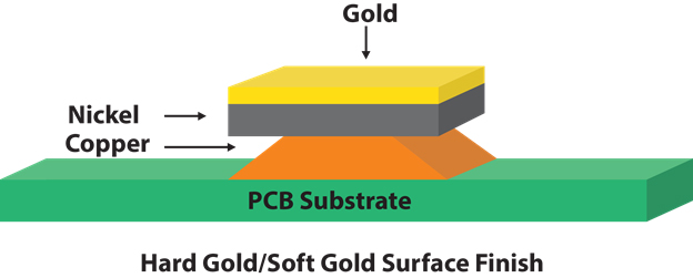
Generally speaking, and with all other factors being equal, Electrolytic Nickel/Gold is the most expensive PCB surface finish. However, some applications do require the Electrolytic Nickel/Gold surface finish.
| Properties of Soft Gold | |
|---|---|
| Properties | Soft Gold |
|
Contact Applications |
Yes |
|
Deposit |
Electrolytic |
|
Exposed Copper |
No |
|
Handling |
Normal |
|
Process Control |
Fair |
|
Process Cost |
High |
|
Required Thermal Cycles |
>2 |
|
Shelf Life |
Long (1+ Years) |
|
SMT |
Flat |
|
Thickness |
99.99% Pure, 24 Karat 30 |
|
Thin Board Finish |
Yes |
| Applications of Soft Gold | |
|---|---|
| Applications | Soft Gold |
|
BGA & μBGA |
Yes |
|
Contact/Connector |
No |
|
Fine Pitch SMT |
Yes |
|
Flip Chip |
Yes |
|
High Reliability |
High |
|
RoHS Compliant |
Yes |
|
Solder Joint Integrity |
Poor |
|
Wire Bonding |
Yes (Au) |
Immersion Silver (also called immersion Ag) is a RoHS compliant (lead-free) surface finish that is an ideal choice for flat surface requirements and fine pitch components with reasonable costs. This surface finish can also replace Immersion Gold over Electroless Nickel (Au/Ni) for most applications. And the thickness ranges from 0.12 to 0.40 μm.
Silver is applied directly to the copper and, unlike ENIG, does not require a diffusion barrier.
It's also an ideal choice for special applications that want to avoid any magnetic materials in the PCB.
It has a decent shelf life of 6 to 12 months, but it can be sensitive to contaminants found in the air and on some surfaces. This makes it critical to have a highly qualified boardhouse to properly control and expedite the board packaging process. This surface finish is also subject to tarnishing, which is something to take into account.
As mentioned above, common applications include flat surface requirements, which may include:
| Immersion Silver | ||
|---|---|---|
| PROS | ||
|
RoHS Compliant |
||
|
Planar |
||
|
Great for Fine Pitch / BGA |
||
|
Cost Effective |
||
|
Highly Stable |
||
|
Simple Processing |
||
|
Very Flat Surface |
||
|
Reworkable |
||
|
Excellent Solderability |
||
| CONS | ||
|
Subject to Tarnishing |
||
|
Silver Metal Whiskering |
||
|
High Friction Coefficient |
||
|
Sensitive to Contaminants |
||
|
Strict Storage and Handling Requirements |
||
|
Welding Issues with Micro-Holes |
||
|
Prone to Electromigration |
||
|
Difficulty with Electric Testing |
||
| Properties of Silver | |
|---|---|
| Characteristics | Silver |
|
Contact Applications |
No |
|
Deposit |
Immersion |
|
Exposed Copper |
No |
|
Handling |
Critical |
|
Process Control |
Fair |
|
Process Cost |
Medium |
|
Required Thermal Cycles |
>2 |
|
Shelf Life |
Medium (9-12 Months)* |
|
SMT |
Flat |
|
Thickness |
6 - 18 µin |
|
Thin Board Finish |
Yes |
*Requires Unique Storage Techniques µin = Microinches
| Applications of Silver | |
|---|---|
| Applications | Silver |
|
BGA & μBGA |
Yes |
|
Contact/Connector |
No |
|
Fine Pitch SMT |
Yes |
|
Flip Chip |
Yes |
|
High Reliability |
Medium/High |
|
RoHS Compliant |
Yes |
|
Solder Joint Integrity |
Excellent |
|
Wire Bonding |
No |
Immersion Tin is a is a RoHS compliant (lead-free) surface finish that is an ideal choice for flat surface requirements and fine pitch components. White Tin (Immersion Tin) is a deposit of a thin layer of Tin on Copper layer of a PCBs. It is not used as often as other surface finishes because not all PCB manufacturers offer it. The flatness of this particular coating makes this an ideal surface finish choice for small geometries and components.
Tin also is the least expensive type of immersion coatings. Although it is an economical choice, it does come with some drawbacks.
Immersion Tin has its advantages, but there are a few disadvantages to using this surface finish. As you may know, Copper and Tin have a strong affinity for one another. This means, over time, diffusion of one metal into the other will occur. It directly impacts the shelf life of the Immersion Tin deposit and ultimately the performance of the ?nish.
Immersion Tin has a limited shelf life, 3-6 months. For the best results assembly (soldering) shall happen during 30 days.
Tin Whiskering is also another downside to using Immersion Tin as a surface finish. The negative effects of tin whiskers growth are well described in industry related literature and topics of several published papers.
The Immersion Tin finish is not very durable, therefore, PCBs with Immersion Tin finish must be handled with caution. It provides a consistently flat surface approximately 20-40 micro inches in thickness.
Immersion Tin has been primarily used as an alternative to a lead-based surface finish. It is also used for its very flat and smooth finish making it ideal for fine geometries and fine pitch surface mount components.
Another reason to use immersion tin is sustainability. Elements that may be difficult to source on a consistent basis are used in other finishes, such as ENIG or HASL. Additionally, it uses less water and chemicals in the application process.
It is also easier to re-work.
As with all of the surface finishes we’ve compared so far, there are a number of advantages and disadvantages. Here are the advantages and disadvantages for Immersion Tin.
Advantages:
Disadvantages:
Here is a full table with some of the pros and cons along with some of the most common uses for the Immersion Tin surface finish.
| Immersion Tin | ||
|---|---|---|
| PROS | ||
|
RoHS Compliant |
||
|
Great for Fine Pitch / BGA |
||
|
Cost Effective |
||
|
Highly Stable |
||
|
Simple Processing |
||
|
Very Flat Surface |
||
|
Reworkable |
||
|
Excellent Solderability |
||
| CONS | ||
|
Subject to Tarnishing |
||
|
Silver Metal Whiskering |
||
|
High Friction Coefficient |
||
|
Sensitive to Contaminants |
||
|
Strict Storage and Handling Requirements |
||
|
Difficulty with Electric Testing |
||
| Properties of White Tin | |
|---|---|
| Properties | White Tin |
|
Contact Applications |
No |
|
Deposit |
Immersion |
|
Exposed Copper |
No |
|
Handling |
Normal |
|
Process Control |
Fair |
|
Process Cost |
Medium |
|
Required Thermal Cycles |
>2 |
|
Shelf Life |
Medium (9-12 Months)* |
|
SMT |
Flat |
|
Thickness |
25 - 60 µin |
|
Thin Board Finish |
Yes |
*Requires Unique Storage Techniques µin = Microinches
| Applications of White Tin | |
|---|---|
| Applications | White Tin |
|
BGA & μBGA |
Yes |
|
Contact/Connector |
No |
|
Fine Pitch SMT |
Yes |
|
Flip Chip |
Yes |
|
High Reliability |
Medium |
|
RoHS Compliant |
Yes |
|
Solder Joint Integrity |
Good |
|
Wire Bonding |
No |
These are the lead-free PCB surface finishes we have available for your PCB order.
For more information, please contact our experts at 1.800.SFC.5143 or get a PCB production quote.
|
Gold Finish |
May be Electrolytic Electroless, or Immersion |
|
- ENIG |
2-5 micro inches. Purpose: To prevent oxidation, extend shelf life, provide a wire bonding surface (when aluminum wire is used), and used to provide an electrically conductive surface on PCBs. Used for solderability when the flatness of the pad is critical. ENIG has shelf life longer then 12 months. |
|
- Hard Gold |
Purpose: “Wear and tear” used for Gold Fingers (minimum 30 micro inches),contacts, keypads soldering (maximum 17 micro inches), to prevent oxidation and extend shelf life. |
|
- Soft Gold |
Purpose: Used for wire bonding (Ultrasonic minimum 2 micro inches/Thermasonic minimum 30 micro inches) and to prevent oxidation and extend shelf life. |
|
Immersion Silver |
Use for solderability purposes (2-10 micro inches). Used for solderability when the flatness of the pad is critical. |
|
Lead Free Solder |
Use for solderability purposes (70-200 micro inches). Used for solderability when the flatness of the pad is not critical. |
|
OSP |
Used for solderability when the flatness of the pad is critical. |
|
White Tin (Immersion Tin) |
Used for solderability when the flatness of the pad is critical. |
San Francisco Circuits specializes in helping you choose the right PCB surface finish. You have a lot of factors to think about like cost, application environment, lead/lead free requirements, shelf life, and so much more! Let us worry about those things and give you the right PCB surface finish.
When it comes to choosing the right type of surface finish, you want to make sure you select the best one for end performance. That’s where you can work with our trusted engineers who have the experience you need to get what’s best for your situation. We look forward to connecting with you!
